DK-DEV-5M570ZN Altera, DK-DEV-5M570ZN Datasheet - Page 96
DK-DEV-5M570ZN
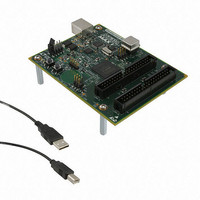
Manufacturer Part Number
DK-DEV-5M570ZN
Description
KIT DEV MAX V 5M570Z
Manufacturer
Altera
Series
MAX® Vr
Type
CPLDr
Datasheets
1.DK-DEV-5M570ZN.pdf
(30 pages)
2.DK-DEV-5M570ZN.pdf
(2 pages)
3.DK-DEV-5M570ZN.pdf
(30 pages)
4.DK-DEV-5M570ZN.pdf
(164 pages)
5.DK-DEV-5M570ZN.pdf
(24 pages)
Specifications of DK-DEV-5M570ZN
Contents
Board, Cable(s), Software and Documentation
Silicon Manufacturer
Altera
Core Architecture
CPLD
Core Sub-architecture
MAX
Silicon Core Number
5M
Silicon Family Name
MAX V
Kit Contents
MAX V CPLD Development Board, USB Cable
Rohs Compliant
Yes
Lead Free Status / RoHS Status
Lead free / RoHS Compliant
For Use With/related Products
5M570ZF256
Lead Free Status / Rohs Status
Compliant
Other names
544-2722
Available stocks
Company
Part Number
Manufacturer
Quantity
Price


6–2
Table 6–1. JTAG Instructions for MAX V Devices (Part 2 of 2)
MAX V Device Handbook
IDCODE
HIGHZ
CLAMP
USER0
USER1
IEEE 1532
instructions
Note to
(1) HIGHZ, CLAMP, and EXTEST instructions do not disable weak pull-up resistors or bus hold features.
JTAG Instruction
Table
(1)
(1)
6–1:
w
You must not issue unsupported JTAG instructions to the MAX V device because this
may put the device into an unknown state, requiring a power cycle to recover device
operation.
For the instruction codes
of the IEEE 1532
instructions, refer to the
IEEE 1532 BSDL Files
page of the Altera
website.
Instruction Code
00 0000 0110
00 0000 1011
00 0000 1010
00 0000 1100
00 0000 1110
Selects the IDCODE register and places it between the TDI and TDO
pins, allowing you to shift the IDCODE register out of the TDO pin
serially.
Places the 1-bit bypass register between the TDI and TDO pins,
which allows the BST data to pass synchronously through target
devices to adjacent devices if the device is operating in normal mode
and tri-stating all the I/O pins.
Places the 1-bit bypass register between the TDI and TDO pins,
which allows the BST data to pass synchronously through target
devices to adjacent devices during normal device operation and
holding I/O pins to a state defined by the data in the boundary-scan
register.
Allows you to define the scan chain between the TDI and TDO pins in
the MAX V logic array. Use this instruction for custom logic and
JTAG interfaces.
Allows you to define the scan chain between the TDI and TDO pins in
the MAX V logic array. Use this instruction for custom logic and
JTAG interfaces.
IEEE 1532 in-system concurrent (ISC) instructions used if
programming a MAX V device through the JTAG port.
Chapter 6: JTAG and In-System Programmability in MAX V Devices
Description
IEEE Std. 1149.1 Boundary-Scan Support
December 2010 Altera Corporation
Related parts for DK-DEV-5M570ZN
Image
Part Number
Description
Manufacturer
Datasheet
Request
R

Part Number:
Description:
KIT DEV ARRIA II GX FPGA 2AGX125
Manufacturer:
Altera
Datasheet:

Part Number:
Description:
KIT DEV CYCLONE III LS EP3CLS200
Manufacturer:
Altera
Datasheet:

Part Number:
Description:
KIT DEV STRATIX IV FPGA 4SE530
Manufacturer:
Altera
Datasheet:

Part Number:
Description:
KIT DEV FPGA 2AGX260 W/6.375G TX
Manufacturer:
Altera
Datasheet:

Part Number:
Description:
KIT DEV STRATIX V FPGA 5SGXEA7
Manufacturer:
Altera
Datasheet:

Part Number:
Description:
KIT DEVELOPMENT STRATIX III
Manufacturer:
Altera
Datasheet:

Part Number:
Description:
KIT DEVELOPMENT STRATIX IV
Manufacturer:
Altera
Datasheet:

Part Number:
Description:
KIT DEV ARRIA GX 1AGX60N
Manufacturer:
Altera
Datasheet:
Part Number:
Description:
KIT STARTER CYCLONE IV GX
Manufacturer:
Altera
Datasheet:
Part Number:
Description:
KIT DEVELOPMENT STRATIX IV
Manufacturer:
Altera
Datasheet:

Part Number:
Description:
CPLD, EP610 Family, ECMOS Process, 300 Gates, 16 Macro Cells, 16 Reg., 16 User I/Os, 5V Supply, 35 Speed Grade, 24DIP
Manufacturer:
Altera Corporation
Datasheet:
Part Number:
Description:
CPLD, EP610 Family, ECMOS Process, 300 Gates, 16 Macro Cells, 16 Reg., 16 User I/Os, 5V Supply, 15 Speed Grade, 24DIP
Manufacturer:
Altera Corporation
Datasheet: