DK-DEV-5M570ZN Altera, DK-DEV-5M570ZN Datasheet - Page 108
DK-DEV-5M570ZN
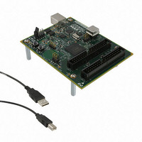
Manufacturer Part Number
DK-DEV-5M570ZN
Description
KIT DEV MAX V 5M570Z
Manufacturer
Altera
Series
MAX® Vr
Type
CPLDr
Datasheets
1.DK-DEV-5M570ZN.pdf
(30 pages)
2.DK-DEV-5M570ZN.pdf
(2 pages)
3.DK-DEV-5M570ZN.pdf
(30 pages)
4.DK-DEV-5M570ZN.pdf
(164 pages)
5.DK-DEV-5M570ZN.pdf
(24 pages)
Specifications of DK-DEV-5M570ZN
Contents
Board, Cable(s), Software and Documentation
Silicon Manufacturer
Altera
Core Architecture
CPLD
Core Sub-architecture
MAX
Silicon Core Number
5M
Silicon Family Name
MAX V
Kit Contents
MAX V CPLD Development Board, USB Cable
Rohs Compliant
Yes
Lead Free Status / RoHS Status
Lead free / RoHS Compliant
For Use With/related Products
5M570ZF256
Lead Free Status / Rohs Status
Compliant
Other names
544-2722
Available stocks
Company
Part Number
Manufacturer
Quantity
Price


7–6
Figure 7–3. UFM Data Register
MAX V Device Handbook
DRDin
UFM Data Register
UFM Program/Erase Control Block
LSB
D0
The UFM data register is 16 bits wide with four control signals: DRSHFT, DRCLK, DRDin,
and DRDout. DRSHFT distinguishes between clock edges that move data serially from
DRDin to DRDout and clock edges that latch parallel data from the UFM sectors. If the
DRSHFT signal is high, a clock edge moves data serially through the registers from
DRDin to DRDout. If the DRSHFT signal is low, a clock edge captures data from the UFM
sector pointed by the address register in parallel. The MSB is the first bit that is seen at
DRDout. The data register DRSHFT signal is also used to enable the UFM for reading
data. When the DRSHFT signal is low, the UFM latches data into the data register.
Figure 7–3
The UFM program/erase control block is used to generate all the control signals
necessary to program and erase the UFM block independently. This block reduces the
number of logic elements (LEs) necessary to implement a UFM controller in the logic
array. It also guarantees correct timing of the control signals to the UFM. A rising edge
on either PROGRAM or ERASE signal causes this control signal block to activate and begin
sequencing through the program or erase cycle. At this point, for a program
instruction, the data currently in the data register is written to the address pointed to
by the address register.
Only sector erase is supported by the UFM. When an ERASE command is executed,
this control block erases the sector whose address is stored in the address register.
When the PROGRAM or ERASE command first activates the program/erase control
block, the BUSY signal will be driven high to indicate an operation in progress in the
UFM. After the program or erase algorithm is completed, the BUSY signal is forced
low.
D1
D2
D3
shows the UFM data register.
D4
D5
D6
16
MAX V UFM Block
D7
Data Register
D8
D9
D10
16
D11
Chapter 7: User Flash Memory in MAX V Devices
D12
D13
January 2011 Altera Corporation
D14
UFM Functional Description
MSB
D15
DRDout
DRCLK
Related parts for DK-DEV-5M570ZN
Image
Part Number
Description
Manufacturer
Datasheet
Request
R

Part Number:
Description:
KIT DEV ARRIA II GX FPGA 2AGX125
Manufacturer:
Altera
Datasheet:

Part Number:
Description:
KIT DEV CYCLONE III LS EP3CLS200
Manufacturer:
Altera
Datasheet:

Part Number:
Description:
KIT DEV STRATIX IV FPGA 4SE530
Manufacturer:
Altera
Datasheet:

Part Number:
Description:
KIT DEV FPGA 2AGX260 W/6.375G TX
Manufacturer:
Altera
Datasheet:

Part Number:
Description:
KIT DEV STRATIX V FPGA 5SGXEA7
Manufacturer:
Altera
Datasheet:

Part Number:
Description:
KIT DEVELOPMENT STRATIX III
Manufacturer:
Altera
Datasheet:

Part Number:
Description:
KIT DEVELOPMENT STRATIX IV
Manufacturer:
Altera
Datasheet:

Part Number:
Description:
KIT DEV ARRIA GX 1AGX60N
Manufacturer:
Altera
Datasheet:
Part Number:
Description:
KIT STARTER CYCLONE IV GX
Manufacturer:
Altera
Datasheet:
Part Number:
Description:
KIT DEVELOPMENT STRATIX IV
Manufacturer:
Altera
Datasheet:

Part Number:
Description:
CPLD, EP610 Family, ECMOS Process, 300 Gates, 16 Macro Cells, 16 Reg., 16 User I/Os, 5V Supply, 35 Speed Grade, 24DIP
Manufacturer:
Altera Corporation
Datasheet:
Part Number:
Description:
CPLD, EP610 Family, ECMOS Process, 300 Gates, 16 Macro Cells, 16 Reg., 16 User I/Os, 5V Supply, 15 Speed Grade, 24DIP
Manufacturer:
Altera Corporation
Datasheet: