DK-DEV-5M570ZN Altera, DK-DEV-5M570ZN Datasheet - Page 83
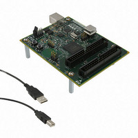
DK-DEV-5M570ZN
Manufacturer Part Number
DK-DEV-5M570ZN
Description
KIT DEV MAX V 5M570Z
Manufacturer
Altera
Series
MAX® Vr
Type
CPLDr
Datasheets
1.DK-DEV-5M570ZN.pdf
(30 pages)
2.DK-DEV-5M570ZN.pdf
(2 pages)
3.DK-DEV-5M570ZN.pdf
(30 pages)
4.DK-DEV-5M570ZN.pdf
(164 pages)
5.DK-DEV-5M570ZN.pdf
(24 pages)
Specifications of DK-DEV-5M570ZN
Contents
Board, Cable(s), Software and Documentation
Silicon Manufacturer
Altera
Core Architecture
CPLD
Core Sub-architecture
MAX
Silicon Core Number
5M
Silicon Family Name
MAX V
Kit Contents
MAX V CPLD Development Board, USB Cable
Rohs Compliant
Yes
Lead Free Status / RoHS Status
Lead free / RoHS Compliant
For Use With/related Products
5M570ZF256
Lead Free Status / Rohs Status
Compliant
Other names
544-2722
Available stocks
Company
Part Number
Manufacturer
Quantity
Price


Chapter 4: Hot Socketing and Power-On Reset in MAX V Devices
Hot-Socketing Feature Implementation in MAX V Devices
Hot-Socketing Feature Implementation in MAX V Devices
Figure 4–1. Hot-Socketing Circuitry for MAX V Devices
December 2010 Altera Corporation
f
1
The hot-socketing feature tri-states the output buffer during the power-up event
(either the V
circuitry generates an internal HOTSCKT signal when either V
the threshold voltage during power up or power down. The HOTSCKT signal cuts off
the output buffer to ensure that no DC current leaks through the pin (except for weak
pull-up leaking). When V
relatively low even after the POR signal is released and device configuration is
complete.
Ensure that V
download has completed.
Figure 4–1
The POR circuit monitors the V
tri-stated until the device has completed its flash memory configuration of the SRAM
logic. The weak pull-up resistor (R) from the I/O pin to V
download to keep the I/O pins from floating. The 3.3-V tolerance control circuit
permits the I/O pins to be driven by 3.3 V before V
and it prevents the I/O pins from driving out when the device is not fully powered or
operational. The hot-socketing circuitry prevents the I/O pins from internally
powering V
powered.
For more information about the 5.0-V tolerance, refer to the
Multi-Voltage Systems
Resistor
Pull-Up
Weak
PAD
shows the circuitry for each I/O and clock pin.
CCIO
CCINT
CCINT
and V
or V
is within the recommended operating range even though SRAM
V
CCIO
chapter.
CCIO
CCINT
CC
power supplies) or power-down event. The hot-socketing
when driven by external signals before the device is
ramps up very slowly during power up, V
CCINT
Input Buffer
to Logic Array
Tolerance
Voltage
Control
and V
CCIO
Output Enable
voltage levels and keeps the I/O pins
CCIO
Hot Socket
Power On
and/or V
Monitor
Reset
CCIO
Using MAX V Devices in
CCINT
is enabled during
CCINT
or V
MAX V Device Handbook
CCIO
CC
are powered,
may still be
is below
4–3
Related parts for DK-DEV-5M570ZN
Image
Part Number
Description
Manufacturer
Datasheet
Request
R

Part Number:
Description:
KIT DEV ARRIA II GX FPGA 2AGX125
Manufacturer:
Altera
Datasheet:

Part Number:
Description:
KIT DEV CYCLONE III LS EP3CLS200
Manufacturer:
Altera
Datasheet:

Part Number:
Description:
KIT DEV STRATIX IV FPGA 4SE530
Manufacturer:
Altera
Datasheet:

Part Number:
Description:
KIT DEV FPGA 2AGX260 W/6.375G TX
Manufacturer:
Altera
Datasheet:

Part Number:
Description:
KIT DEV STRATIX V FPGA 5SGXEA7
Manufacturer:
Altera
Datasheet:

Part Number:
Description:
KIT DEVELOPMENT STRATIX III
Manufacturer:
Altera
Datasheet:

Part Number:
Description:
KIT DEVELOPMENT STRATIX IV
Manufacturer:
Altera
Datasheet:

Part Number:
Description:
KIT DEV ARRIA GX 1AGX60N
Manufacturer:
Altera
Datasheet:
Part Number:
Description:
KIT STARTER CYCLONE IV GX
Manufacturer:
Altera
Datasheet:
Part Number:
Description:
KIT DEVELOPMENT STRATIX IV
Manufacturer:
Altera
Datasheet:

Part Number:
Description:
CPLD, EP610 Family, ECMOS Process, 300 Gates, 16 Macro Cells, 16 Reg., 16 User I/Os, 5V Supply, 35 Speed Grade, 24DIP
Manufacturer:
Altera Corporation
Datasheet:
Part Number:
Description:
CPLD, EP610 Family, ECMOS Process, 300 Gates, 16 Macro Cells, 16 Reg., 16 User I/Os, 5V Supply, 15 Speed Grade, 24DIP
Manufacturer:
Altera Corporation
Datasheet: