DK-DEV-5M570ZN Altera, DK-DEV-5M570ZN Datasheet - Page 123
DK-DEV-5M570ZN
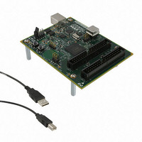
Manufacturer Part Number
DK-DEV-5M570ZN
Description
KIT DEV MAX V 5M570Z
Manufacturer
Altera
Series
MAX® Vr
Type
CPLDr
Datasheets
1.DK-DEV-5M570ZN.pdf
(30 pages)
2.DK-DEV-5M570ZN.pdf
(2 pages)
3.DK-DEV-5M570ZN.pdf
(30 pages)
4.DK-DEV-5M570ZN.pdf
(164 pages)
5.DK-DEV-5M570ZN.pdf
(24 pages)
Specifications of DK-DEV-5M570ZN
Contents
Board, Cable(s), Software and Documentation
Silicon Manufacturer
Altera
Core Architecture
CPLD
Core Sub-architecture
MAX
Silicon Core Number
5M
Silicon Family Name
MAX V
Kit Contents
MAX V CPLD Development Board, USB Cable
Rohs Compliant
Yes
Lead Free Status / RoHS Status
Lead free / RoHS Compliant
For Use With/related Products
5M570ZF256
Lead Free Status / Rohs Status
Compliant
Other names
544-2722
Available stocks
Company
Part Number
Manufacturer
Quantity
Price


Chapter 7: User Flash Memory in MAX V Devices
Software Support for UFM Block
Figure 7–16. Random Address Read Sequence
Figure 7–17. Sequential Read Sequence
January 2011 Altera Corporation
S – Start Condition
Sr – Repeated Start
P – Stop Condition
A – Acknowledge
S
S – Start Condition
Sr – Repeated Start
P – Stop Condition
A – Acknowledge
S
Address
Slave
Address
Slave
‘0’ (write)
Random Address Read
Random address read operation allows the master to select any byte location for a
read operation. The master first performs a “dummy” write operation by sending the
start condition, slave address, and byte address of the location it wishes to read. After
the ALTUFM_I2C megafunction acknowledges the slave and byte address, the master
generates a repeated start condition, the slave address, and the R/W bit is set to 1. The
ALTUFM_I2C megafunction then responds with acknowledge and sends the 8-bit
data requested. The master then generates a stop condition.
random address read sequence.
Sequential Read
Sequential read operation can be initiated by either the current address read operation
or the random address read operation. Instead of sending a stop condition after the
slave has transmitted one byte of data to the master, the master acknowledges that
byte and sends additional clock pulses (on the SCL line) for the slave to transmit data
bytes from consecutive byte addresses. The operation is terminated when the master
generates a stop condition instead of responding with an acknowledge.
shows the sequential read sequence.
R/W
‘0’ (write)
R/W
A
A
Address
Byte
Address
Byte
A
Sr
A
Address
Sr
Slave
Address
Slave
‘1’ (read)
R/W
‘1’ (read)
A
R/W
Data (n - bytes) + Acknowledgment (n - 1 bytes)
Data
A
From Master to Slave
From Slave to Master
From Master to Slave
From Slave to Master
A
Figure 7–16
Data
…
MAX V Device Handbook
Data
Figure 7–17
shows the
P
P
7–21
Related parts for DK-DEV-5M570ZN
Image
Part Number
Description
Manufacturer
Datasheet
Request
R

Part Number:
Description:
KIT DEV ARRIA II GX FPGA 2AGX125
Manufacturer:
Altera
Datasheet:

Part Number:
Description:
KIT DEV CYCLONE III LS EP3CLS200
Manufacturer:
Altera
Datasheet:

Part Number:
Description:
KIT DEV STRATIX IV FPGA 4SE530
Manufacturer:
Altera
Datasheet:

Part Number:
Description:
KIT DEV FPGA 2AGX260 W/6.375G TX
Manufacturer:
Altera
Datasheet:

Part Number:
Description:
KIT DEV STRATIX V FPGA 5SGXEA7
Manufacturer:
Altera
Datasheet:

Part Number:
Description:
KIT DEVELOPMENT STRATIX III
Manufacturer:
Altera
Datasheet:

Part Number:
Description:
KIT DEVELOPMENT STRATIX IV
Manufacturer:
Altera
Datasheet:

Part Number:
Description:
KIT DEV ARRIA GX 1AGX60N
Manufacturer:
Altera
Datasheet:
Part Number:
Description:
KIT STARTER CYCLONE IV GX
Manufacturer:
Altera
Datasheet:
Part Number:
Description:
KIT DEVELOPMENT STRATIX IV
Manufacturer:
Altera
Datasheet:

Part Number:
Description:
CPLD, EP610 Family, ECMOS Process, 300 Gates, 16 Macro Cells, 16 Reg., 16 User I/Os, 5V Supply, 35 Speed Grade, 24DIP
Manufacturer:
Altera Corporation
Datasheet:
Part Number:
Description:
CPLD, EP610 Family, ECMOS Process, 300 Gates, 16 Macro Cells, 16 Reg., 16 User I/Os, 5V Supply, 15 Speed Grade, 24DIP
Manufacturer:
Altera Corporation
Datasheet: