DK-DEV-5M570ZN Altera, DK-DEV-5M570ZN Datasheet - Page 46
DK-DEV-5M570ZN
Manufacturer Part Number
DK-DEV-5M570ZN
Description
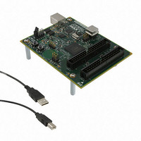
KIT DEV MAX V 5M570Z
Manufacturer
Altera
Series
MAX® Vr
Type
CPLDr
Datasheets
1.DK-DEV-5M570ZN.pdf
(30 pages)
2.DK-DEV-5M570ZN.pdf
(2 pages)
3.DK-DEV-5M570ZN.pdf
(30 pages)
4.DK-DEV-5M570ZN.pdf
(164 pages)
5.DK-DEV-5M570ZN.pdf
(24 pages)
Specifications of DK-DEV-5M570ZN
Contents
Board, Cable(s), Software and Documentation
Silicon Manufacturer
Altera
Core Architecture
CPLD
Core Sub-architecture
MAX
Silicon Core Number
5M
Silicon Family Name
MAX V
Kit Contents
MAX V CPLD Development Board, USB Cable
Rohs Compliant
Yes
Lead Free Status / RoHS Status
Lead free / RoHS Compliant
For Use With/related Products
5M570ZF256
Lead Free Status / Rohs Status
Compliant
Other names
544-2722
Available stocks
Company
Part Number
Manufacturer
Quantity
Price


2–34
MAX V Device Handbook
Slew-Rate Control
Open-Drain Output
Programmable Ground Pins
Bus-Hold
1
The output buffer for each MAX V device I/O pin has a programmable output
slew-rate control that can be configured for low noise or high-speed performance. A
faster slew rate provides high-speed transitions for high-performance systems.
However, these fast transitions may introduce noise transients into the system. A slow
slew rate reduces system noise, but adds a nominal output delay to rising and falling
edges. The lower the voltage standard (for example, 1.8-V LVTTL) the larger the
output delay when slow slew is enabled. Each I/O pin has an individual slew-rate
control, allowing you to specify the slew rate on a pin-by-pin basis. The slew-rate
control affects both the rising and falling edges. If no slew-rate control is specified, the
Quartus II software defaults to a fast slew rate.
The slew-rate control feature can be used simultaneously with the programmable
drive strength feature.
MAX V devices provide an optional open-drain (equivalent to open-collector) output
for each I/O pin. This open-drain output enables the device to provide system-level
control signals (for example, interrupt and write enable signals) that can be asserted
by any of several devices. This output can also provide an additional wired-OR plane.
Each unused I/O pin on MAX V devices can be used as an additional ground pin.
This programmable ground feature does not require the use of the associated LEs in
the device. In the Quartus II software, unused pins can be set as programmable GND
on a global default basis or they can be individually assigned. Unused pins also have
the option of being set as tri-stated input pins.
Each MAX V device I/O pin provides an optional bus-hold feature. The bus-hold
circuitry can hold the signal on an I/O pin at its last-driven state. Because the bus-
hold feature holds the last-driven state of the pin until the next input signal is present,
an external pull-up or pull-down resistor is not necessary to hold a signal level when
the bus is tri-stated.
The bus-hold circuitry also pulls un-driven pins away from the input threshold
voltage where noise can cause unintended high-frequency switching. You can select
this feature individually for each I/O pin. The bus-hold output will drive no higher
than V
device cannot use the programmable pull-up option.
The bus-hold circuitry is only active after the device has fully initialized. The bus-hold
circuit captures the value on the pin present at the moment user mode is entered.
CCIO
to prevent overdriving signals. If the bus-hold feature is enabled, the
December 2010 Altera Corporation
Chapter 2: MAX V Architecture
I/O Structure
Related parts for DK-DEV-5M570ZN
Image
Part Number
Description
Manufacturer
Datasheet
Request
R

Part Number:
Description:
KIT DEV ARRIA II GX FPGA 2AGX125
Manufacturer:
Altera
Datasheet:

Part Number:
Description:
KIT DEV CYCLONE III LS EP3CLS200
Manufacturer:
Altera
Datasheet:

Part Number:
Description:
KIT DEV STRATIX IV FPGA 4SE530
Manufacturer:
Altera
Datasheet:

Part Number:
Description:
KIT DEV FPGA 2AGX260 W/6.375G TX
Manufacturer:
Altera
Datasheet:

Part Number:
Description:
KIT DEV STRATIX V FPGA 5SGXEA7
Manufacturer:
Altera
Datasheet:

Part Number:
Description:
KIT DEVELOPMENT STRATIX III
Manufacturer:
Altera
Datasheet:

Part Number:
Description:
KIT DEVELOPMENT STRATIX IV
Manufacturer:
Altera
Datasheet:

Part Number:
Description:
KIT DEV ARRIA GX 1AGX60N
Manufacturer:
Altera
Datasheet:
Part Number:
Description:
KIT STARTER CYCLONE IV GX
Manufacturer:
Altera
Datasheet:
Part Number:
Description:
KIT DEVELOPMENT STRATIX IV
Manufacturer:
Altera
Datasheet:

Part Number:
Description:
CPLD, EP610 Family, ECMOS Process, 300 Gates, 16 Macro Cells, 16 Reg., 16 User I/Os, 5V Supply, 35 Speed Grade, 24DIP
Manufacturer:
Altera Corporation
Datasheet:
Part Number:
Description:
CPLD, EP610 Family, ECMOS Process, 300 Gates, 16 Macro Cells, 16 Reg., 16 User I/Os, 5V Supply, 15 Speed Grade, 24DIP
Manufacturer:
Altera Corporation
Datasheet: