DK-DEV-5M570ZN Altera, DK-DEV-5M570ZN Datasheet - Page 101
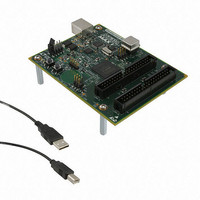
DK-DEV-5M570ZN
Manufacturer Part Number
DK-DEV-5M570ZN
Description
KIT DEV MAX V 5M570Z
Manufacturer
Altera
Series
MAX® Vr
Type
CPLDr
Datasheets
1.DK-DEV-5M570ZN.pdf
(30 pages)
2.DK-DEV-5M570ZN.pdf
(2 pages)
3.DK-DEV-5M570ZN.pdf
(30 pages)
4.DK-DEV-5M570ZN.pdf
(164 pages)
5.DK-DEV-5M570ZN.pdf
(24 pages)
Specifications of DK-DEV-5M570ZN
Contents
Board, Cable(s), Software and Documentation
Silicon Manufacturer
Altera
Core Architecture
CPLD
Core Sub-architecture
MAX
Silicon Core Number
5M
Silicon Family Name
MAX V
Kit Contents
MAX V CPLD Development Board, USB Cable
Rohs Compliant
Yes
Lead Free Status / RoHS Status
Lead free / RoHS Compliant
For Use With/related Products
5M570ZF256
Lead Free Status / Rohs Status
Compliant
Other names
544-2722
Available stocks
Company
Part Number
Manufacturer
Quantity
Price


Chapter 6: JTAG and In-System Programmability in MAX V Devices
In-System Programmability
Table 6–4. Family Programming Times for MAX V Devices
December 2010 Altera Corporation
Erase + Program (1 MHz)
Erase + Program (10 MHz)
Verify (1 MHz)
Verify (10 MHz)
Complete Program Cycle (1 MHz)
Complete Program Cycle (10 MHz)
Notes to
(1) Not applicable to T144 package of the 5M240Z device.
(2) Only applicable to T144 package of the 5M240Z device.
(3) Not applicable to F324 package of the 5M1270Z device.
(4) Only applicable to F324 package of the 5M1270Z device.
Table
User Flash Memory Programming
In-System Programming Clamp
Description
6–4:
f
A stand-alone verification of a programmed pattern involves only steps 1, 2, 5, and 6.
These steps are automatically executed by third-party programmers, the Quartus II
software, or the Jam STAPL and Jam Byte-Code Players.
Table 6–4
execute the algorithm vectors in hardware. Because of data processing and data
transfer limitations, software-based programming tools used with download cables
are slightly slower.
The Quartus II software (with the use of .pof, .jam, or .jbc files) supports
programming of the UFM block independent of the logic array design pattern stored
in the CFM block. This allows updating or reading UFM contents through ISP without
altering the current logic array design, or vice versa. By default, these programming
files and methods program the entire flash memory contents, which includes the CFM
block and UFM contents. The stand-alone embedded Jam STAPL Player and Jam
Byte-Code Player provide action commands for programming or reading the entire
flash memory (UFM and CFM together) or each independently.
For more information, refer to
Device
By default, the IEEE 1532 instruction used for entering ISP automatically tri-states all
I/O pins with weak pull-up resistors for the duration of the ISP sequence. However,
some systems may require certain pins on MAX V devices to maintain a specific DC
logic level during an in-field update. For these systems, you can use the optional in-
system programming clamp instruction in the MAX V circuitry to control I/O
Programming.
lists the programming times for MAX V devices with in-circuit testers to
5M240Z
5M160Z/
5M40Z/
5M80Z/
1.72
1.65
0.09
0.01
1.81
1.66
(1)
5M240Z
2.16
1.99
0.17
0.02
2.33
2.01
(2)
AN 425: Using the Command-Line Jam STAPL Solution for
5M570Z
2.16
1.99
0.17
0.02
2.33
2.01
5M1270Z
2.90
2.58
0.30
0.03
3.20
2.61
(3)
5M1270Z
3.92
3.40
0.49
0.05
4.41
3.45
MAX V Device Handbook
(4)
5M2210Z
3.92
3.40
0.05
0.49
4.41
3.45
6–7
Unit
sec
sec
sec
sec
sec
sec
Related parts for DK-DEV-5M570ZN
Image
Part Number
Description
Manufacturer
Datasheet
Request
R

Part Number:
Description:
KIT DEV ARRIA II GX FPGA 2AGX125
Manufacturer:
Altera
Datasheet:

Part Number:
Description:
KIT DEV CYCLONE III LS EP3CLS200
Manufacturer:
Altera
Datasheet:

Part Number:
Description:
KIT DEV STRATIX IV FPGA 4SE530
Manufacturer:
Altera
Datasheet:

Part Number:
Description:
KIT DEV FPGA 2AGX260 W/6.375G TX
Manufacturer:
Altera
Datasheet:

Part Number:
Description:
KIT DEV STRATIX V FPGA 5SGXEA7
Manufacturer:
Altera
Datasheet:

Part Number:
Description:
KIT DEVELOPMENT STRATIX III
Manufacturer:
Altera
Datasheet:

Part Number:
Description:
KIT DEVELOPMENT STRATIX IV
Manufacturer:
Altera
Datasheet:

Part Number:
Description:
KIT DEV ARRIA GX 1AGX60N
Manufacturer:
Altera
Datasheet:
Part Number:
Description:
KIT STARTER CYCLONE IV GX
Manufacturer:
Altera
Datasheet:
Part Number:
Description:
KIT DEVELOPMENT STRATIX IV
Manufacturer:
Altera
Datasheet:

Part Number:
Description:
CPLD, EP610 Family, ECMOS Process, 300 Gates, 16 Macro Cells, 16 Reg., 16 User I/Os, 5V Supply, 35 Speed Grade, 24DIP
Manufacturer:
Altera Corporation
Datasheet:
Part Number:
Description:
CPLD, EP610 Family, ECMOS Process, 300 Gates, 16 Macro Cells, 16 Reg., 16 User I/Os, 5V Supply, 15 Speed Grade, 24DIP
Manufacturer:
Altera Corporation
Datasheet: