DK-DEV-5M570ZN Altera, DK-DEV-5M570ZN Datasheet - Page 154
DK-DEV-5M570ZN
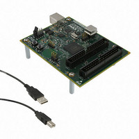
Manufacturer Part Number
DK-DEV-5M570ZN
Description
KIT DEV MAX V 5M570Z
Manufacturer
Altera
Series
MAX® Vr
Type
CPLDr
Datasheets
1.DK-DEV-5M570ZN.pdf
(30 pages)
2.DK-DEV-5M570ZN.pdf
(2 pages)
3.DK-DEV-5M570ZN.pdf
(30 pages)
4.DK-DEV-5M570ZN.pdf
(164 pages)
5.DK-DEV-5M570ZN.pdf
(24 pages)
Specifications of DK-DEV-5M570ZN
Contents
Board, Cable(s), Software and Documentation
Silicon Manufacturer
Altera
Core Architecture
CPLD
Core Sub-architecture
MAX
Silicon Core Number
5M
Silicon Family Name
MAX V
Kit Contents
MAX V CPLD Development Board, USB Cable
Rohs Compliant
Yes
Lead Free Status / RoHS Status
Lead free / RoHS Compliant
For Use With/related Products
5M570ZF256
Lead Free Status / Rohs Status
Compliant
Other names
544-2722
Available stocks
Company
Part Number
Manufacturer
Quantity
Price


8–8
MAX V Device Handbook
SAMPLE/PRELOAD Instruction Mode
f
The TDO pin is tri-stated in all states except the SHIFT_IR and SHIFT_DR states. The TDO
pin is activated at the first falling edge of TCK after entering either of the shift states
and is tri-stated at the first falling edge of TCK after leaving either of the shift states.
When the SHIFT_IR state is activated, TDO is no longer tri-stated, and the initial state of
the instruction register is shifted out on the falling edge of TCK. TDO continues to shift
out the contents of the instruction register as long as the SHIFT_IR state is active. The
TAP controller remains in the SHIFT_IR state as long as TMS remains low.
During the SHIFT_IR state, an instruction code is entered by shifting data on the TDI
pin on the rising edge of TCK. You must clock the last bit of the OPCODE at the same time
that the next state, EXIT1_IR, is activated; EXIT1_IR is entered by clocking a logic high
on TMS. After in the EXIT1_IR state, TDO becomes tri-stated again. TDO is always
tri-stated except in the SHIFT_IR and SHIFT_DR states. After an instruction code is
entered correctly, the TAP controller advances to perform the serial shifting of test
data in one of three modes (SAMPLE/PRELOAD, EXTEST, or BYPASS).
For MAX V devices, there are weak pull-up resistors for TDI and TMS, and pull-down
resistors for TCK. However, in a JTAG chain, there might be some devices that do not
have internal pull-up or pull-down resistors. In this case, Altera recommends pulling
the TMS pin high (through an external 10-k resistor), and pulling TCK low (through an
external 1-k resistor) during BST or in-system programmability (ISP) to prevent the
TAP controller from going into an unintended state. Pulling-up the TDI signal
externally for the MAX V device is optional.
For more information about the pull-up and pull-down resistors, refer to
AN 100: In-System Programmability
SAMPLE/PRELOAD instruction mode allows you to take a snapshot of device data
without interrupting normal device operation. However, SAMPLE/PRELOAD instruction
mode is most often used to preload the test data into the update registers before
loading the EXTEST instruction.
During the capture phase, multiplexers preceding the capture registers select the
active device data signals and clocked data into the capture registers. The
multiplexers at the outputs of the update registers also select active device data to
prevent functional interruptions to the device.
During the shift phase, the boundary-scan shift register is formed by clocking data
through capture registers around the device periphery and then out of the TDO pin.
New test data can simultaneously be shifted into TDI and replace the contents of the
capture registers. During the update phase, data in the capture registers is transferred
to the update registers.You can then use this data in EXTEST instruction mode. For
more information, refer to
“EXTEST Instruction Mode” on page
Guidelines.
Chapter 8: JTAG Boundary-Scan Testing in MAX V Devices
IEEE Std. 1149.1 BST Operation Control
December 2010 Altera Corporation
8–10.
Related parts for DK-DEV-5M570ZN
Image
Part Number
Description
Manufacturer
Datasheet
Request
R

Part Number:
Description:
KIT DEV ARRIA II GX FPGA 2AGX125
Manufacturer:
Altera
Datasheet:

Part Number:
Description:
KIT DEV CYCLONE III LS EP3CLS200
Manufacturer:
Altera
Datasheet:

Part Number:
Description:
KIT DEV STRATIX IV FPGA 4SE530
Manufacturer:
Altera
Datasheet:

Part Number:
Description:
KIT DEV FPGA 2AGX260 W/6.375G TX
Manufacturer:
Altera
Datasheet:

Part Number:
Description:
KIT DEV STRATIX V FPGA 5SGXEA7
Manufacturer:
Altera
Datasheet:

Part Number:
Description:
KIT DEVELOPMENT STRATIX III
Manufacturer:
Altera
Datasheet:

Part Number:
Description:
KIT DEVELOPMENT STRATIX IV
Manufacturer:
Altera
Datasheet:

Part Number:
Description:
KIT DEV ARRIA GX 1AGX60N
Manufacturer:
Altera
Datasheet:
Part Number:
Description:
KIT STARTER CYCLONE IV GX
Manufacturer:
Altera
Datasheet:
Part Number:
Description:
KIT DEVELOPMENT STRATIX IV
Manufacturer:
Altera
Datasheet:

Part Number:
Description:
CPLD, EP610 Family, ECMOS Process, 300 Gates, 16 Macro Cells, 16 Reg., 16 User I/Os, 5V Supply, 35 Speed Grade, 24DIP
Manufacturer:
Altera Corporation
Datasheet:
Part Number:
Description:
CPLD, EP610 Family, ECMOS Process, 300 Gates, 16 Macro Cells, 16 Reg., 16 User I/Os, 5V Supply, 15 Speed Grade, 24DIP
Manufacturer:
Altera Corporation
Datasheet: