DK-DEV-5M570ZN Altera, DK-DEV-5M570ZN Datasheet - Page 147
DK-DEV-5M570ZN
Manufacturer Part Number
DK-DEV-5M570ZN
Description
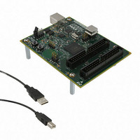
KIT DEV MAX V 5M570Z
Manufacturer
Altera
Series
MAX® Vr
Type
CPLDr
Datasheets
1.DK-DEV-5M570ZN.pdf
(30 pages)
2.DK-DEV-5M570ZN.pdf
(2 pages)
3.DK-DEV-5M570ZN.pdf
(30 pages)
4.DK-DEV-5M570ZN.pdf
(164 pages)
5.DK-DEV-5M570ZN.pdf
(24 pages)
Specifications of DK-DEV-5M570ZN
Contents
Board, Cable(s), Software and Documentation
Silicon Manufacturer
Altera
Core Architecture
CPLD
Core Sub-architecture
MAX
Silicon Core Number
5M
Silicon Family Name
MAX V
Kit Contents
MAX V CPLD Development Board, USB Cable
Rohs Compliant
Yes
Lead Free Status / RoHS Status
Lead free / RoHS Compliant
For Use With/related Products
5M570ZF256
Lead Free Status / Rohs Status
Compliant
Other names
544-2722
Available stocks
Company
Part Number
Manufacturer
Quantity
Price


MV51008-1.0
© 2010 Altera Corporation. All rights reserved. ALTERA, ARRIA, CYCLONE, HARDCOPY, MAX, MEGACORE, NIOS, QUARTUS and STRATIX are Reg. U.S. Pat. & Tm. Off.
and/or trademarks of Altera Corporation in the U.S. and other countries. All other trademarks and service marks are the property of their respective holders as described at
www.altera.com/common/legal.html. Altera warrants performance of its semiconductor products to current specifications in accordance with Altera’s standard warranty, but
reserves the right to make changes to any products and services at any time without notice. Altera assumes no responsibility or liability arising out of the application or use of any
information, product, or service described herein except as expressly agreed to in writing by Altera. Altera customers are advised to obtain the latest version of device
specifications before relying on any published information and before placing orders for products or services.
MAX V Device Handbook
December 2010
December 2010
MV51008-1.0
This chapter describes the IEEE Std.1149.1 (JTAG) boundary-scan testing for Altera
MAX
provides a cost-effective and efficient way to test systems that contain devices with
tight lead spacing. Circuit boards with Altera and other IEEE Std. 1149.1-compliant
devices can use EXTEST, SAMPLE/PRELOAD, and BYPASS modes to create serial patterns
that internally test the pin connections between devices and check device operation.
As PCBs become more complex, the requirement for thorough testing becomes
increasingly important. Advances in surface-mount packaging and PCB
manufacturing have resulted in smaller boards, making traditional test methods (for
example, external test probes and “bed-of-nails” test fixtures) harder to implement.
As a result, cost savings from PCB space reductions are sometimes offset by cost
increases in traditional testing methods.
In the 1980s, JTAG developed a specification for boundary-scan testing that was later
standardized as the IEEE Std. 1149.1 specification. This boundary-scan test (BST)
architecture offers the capability to efficiently test components on PCBs with tight
lead spacing.
BST architecture can test pin connections without using physical test probes and
capture functional data while a device is operating normally. Boundary-scan cells
(BSCs) in a device can force signals onto pins, or capture data from pin or core logic
signals. Forced test data is serially shifted into the BSCs. Captured data is serially
shifted out and externally compared to expected results.
Figure 8–1
Figure 8–1. IEEE Std. 1149.1 Boundary-Scan Testing
This chapter describes the following topics:
■
■
■
■
■
“IEEE Std. 1149.1 BST Architecture” on page 8–2
“IEEE Std. 1149.1 Boundary-Scan Register” on page 8–3
“IEEE Std. 1149.1 BST Operation Control” on page 8–6
“I/O Voltage Support in the JTAG Chain” on page 8–13
“Boundary-Scan Test for Programmed Devices” on page 8–14
®
V devices. The IEEE Std. 1149.1 BST circuitry available in MAX V devices
shows the concept of boundary-scan testing.
Serial
Data In
8. JTAG Boundary-Scan Testing in MAX V
JTAG Device 1
Boundary-Scan Cell
Logic
Core
IC
Interconnection
to Be Tested
Pin Signal
JTAG Device 2
Logic
Core
Serial
Data Out
Devices
Subscribe
®
Related parts for DK-DEV-5M570ZN
Image
Part Number
Description
Manufacturer
Datasheet
Request
R

Part Number:
Description:
KIT DEV ARRIA II GX FPGA 2AGX125
Manufacturer:
Altera
Datasheet:

Part Number:
Description:
KIT DEV CYCLONE III LS EP3CLS200
Manufacturer:
Altera
Datasheet:

Part Number:
Description:
KIT DEV STRATIX IV FPGA 4SE530
Manufacturer:
Altera
Datasheet:

Part Number:
Description:
KIT DEV FPGA 2AGX260 W/6.375G TX
Manufacturer:
Altera
Datasheet:

Part Number:
Description:
KIT DEV STRATIX V FPGA 5SGXEA7
Manufacturer:
Altera
Datasheet:

Part Number:
Description:
KIT DEVELOPMENT STRATIX III
Manufacturer:
Altera
Datasheet:

Part Number:
Description:
KIT DEVELOPMENT STRATIX IV
Manufacturer:
Altera
Datasheet:

Part Number:
Description:
KIT DEV ARRIA GX 1AGX60N
Manufacturer:
Altera
Datasheet:
Part Number:
Description:
KIT STARTER CYCLONE IV GX
Manufacturer:
Altera
Datasheet:
Part Number:
Description:
KIT DEVELOPMENT STRATIX IV
Manufacturer:
Altera
Datasheet:

Part Number:
Description:
CPLD, EP610 Family, ECMOS Process, 300 Gates, 16 Macro Cells, 16 Reg., 16 User I/Os, 5V Supply, 35 Speed Grade, 24DIP
Manufacturer:
Altera Corporation
Datasheet:
Part Number:
Description:
CPLD, EP610 Family, ECMOS Process, 300 Gates, 16 Macro Cells, 16 Reg., 16 User I/Os, 5V Supply, 15 Speed Grade, 24DIP
Manufacturer:
Altera Corporation
Datasheet: