DK-DEV-5M570ZN Altera, DK-DEV-5M570ZN Datasheet - Page 106
DK-DEV-5M570ZN
Manufacturer Part Number
DK-DEV-5M570ZN
Description
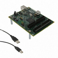
KIT DEV MAX V 5M570Z
Manufacturer
Altera
Series
MAX® Vr
Type
CPLDr
Datasheets
1.DK-DEV-5M570ZN.pdf
(30 pages)
2.DK-DEV-5M570ZN.pdf
(2 pages)
3.DK-DEV-5M570ZN.pdf
(30 pages)
4.DK-DEV-5M570ZN.pdf
(164 pages)
5.DK-DEV-5M570ZN.pdf
(24 pages)
Specifications of DK-DEV-5M570ZN
Contents
Board, Cable(s), Software and Documentation
Silicon Manufacturer
Altera
Core Architecture
CPLD
Core Sub-architecture
MAX
Silicon Core Number
5M
Silicon Family Name
MAX V
Kit Contents
MAX V CPLD Development Board, USB Cable
Rohs Compliant
Yes
Lead Free Status / RoHS Status
Lead free / RoHS Compliant
For Use With/related Products
5M570ZF256
Lead Free Status / Rohs Status
Compliant
Other names
544-2722
Available stocks
Company
Part Number
Manufacturer
Quantity
Price


7–4
Table 7–4. UFM Interface Signals (Part 2 of 2)
MAX V Device Handbook
PROGRAM
ERASE
OSC_ENA
DRDout
BUSY
OSC
RTP_BUSY
Port Name
f
Port Type
Output
Output
Output
Output
Input
Input
Input
For more information about the interaction between the UFM block and the logic
array of MAX V devices, refer to the
Signal that initiates a program sequence. On the rising edge, the data in the data register is
written to the address pointed to by the address register. The BUSY signal asserts until the
program sequence is completed.
Signal that initiates an erase sequence. On a rising edge, the memory sector indicated by
the MSB of the address register is erased. The BUSY signal asserts until the erase sequence
is completed.
This signal turns on the internal oscillator in the UFM block. It is required when the OSC
output is used, but optional otherwise. If OSC_ENA is driven high, the internal oscillator is
enabled and the OSC output will toggle. If OSC_ENA is driven low, the internal oscillator is
disabled and the OSC output drives constant high.
Serial output of the data register. Each time the DRCLK signal is applied, a new value is
available. The DRDout data depends on the DRSHFT signal. When the DRSHFT signal is high,
DRDout contains the new value that is shifted into the MSB of the data register. If DRSHFT is
low, DRDout contains the MSB of the memory location read into the data register.
Signal that indicates when the memory is BUSY performing a PROGRAM or ERASE
instruction. When it is high, the address and data register should not be clocked. The new
PROGRAM or ERASE instruction is not executed until the BUSY signal is deasserted.
Output of the internal oscillator. It can be used to generate a clock to control user logic with
the UFM. It requires an OSC_ENA input to produce an output.
This output signal is optional and only needed if the real-time ISP feature is used. The signal
is asserted high during real-time ISP and stays in the RUN_STATE for 500 ms before
initiating real-time ISP to allow for the final read/erase/write operation. No read, write,
erase, or address and data shift operations are allowed to be issued after the RTP_BUSY
signal goes high. The data and address registers do not retain the contents of the last read
or write operation for the UFM block during real-time ISP.
MAX V Device Architecture
Description
Chapter 7: User Flash Memory in MAX V Devices
January 2011 Altera Corporation
chapter.
UFM Functional Description
Related parts for DK-DEV-5M570ZN
Image
Part Number
Description
Manufacturer
Datasheet
Request
R

Part Number:
Description:
KIT DEV ARRIA II GX FPGA 2AGX125
Manufacturer:
Altera
Datasheet:

Part Number:
Description:
KIT DEV CYCLONE III LS EP3CLS200
Manufacturer:
Altera
Datasheet:

Part Number:
Description:
KIT DEV STRATIX IV FPGA 4SE530
Manufacturer:
Altera
Datasheet:

Part Number:
Description:
KIT DEV FPGA 2AGX260 W/6.375G TX
Manufacturer:
Altera
Datasheet:

Part Number:
Description:
KIT DEV STRATIX V FPGA 5SGXEA7
Manufacturer:
Altera
Datasheet:

Part Number:
Description:
KIT DEVELOPMENT STRATIX III
Manufacturer:
Altera
Datasheet:

Part Number:
Description:
KIT DEVELOPMENT STRATIX IV
Manufacturer:
Altera
Datasheet:

Part Number:
Description:
KIT DEV ARRIA GX 1AGX60N
Manufacturer:
Altera
Datasheet:
Part Number:
Description:
KIT STARTER CYCLONE IV GX
Manufacturer:
Altera
Datasheet:
Part Number:
Description:
KIT DEVELOPMENT STRATIX IV
Manufacturer:
Altera
Datasheet:

Part Number:
Description:
CPLD, EP610 Family, ECMOS Process, 300 Gates, 16 Macro Cells, 16 Reg., 16 User I/Os, 5V Supply, 35 Speed Grade, 24DIP
Manufacturer:
Altera Corporation
Datasheet:
Part Number:
Description:
CPLD, EP610 Family, ECMOS Process, 300 Gates, 16 Macro Cells, 16 Reg., 16 User I/Os, 5V Supply, 15 Speed Grade, 24DIP
Manufacturer:
Altera Corporation
Datasheet: