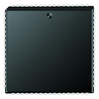
PIC18F6680-I/L Microchip Technology, PIC18F6680-I/L Datasheet - Page 352

PIC18F6680-I/L
Manufacturer Part Number
PIC18F6680-I/L
Description
Microcontrollers (MCU) 64KB 3328 RAM 52 I/O
Manufacturer
Microchip Technology
Datasheet
1.PCM18XK1.pdf
(496 pages)
Specifications of PIC18F6680-I/L
Processor Series
PIC18F
Core
PIC
Data Bus Width
8 bit
Data Ram Size
3.25 KB
Interface Type
I2C/SPI/AUSART/CAN
Maximum Clock Frequency
40 MHz
Number Of Programmable I/os
53
Number Of Timers
5
Operating Supply Voltage
4.2 V to 5.5 V
Maximum Operating Temperature
+ 85 C
Mounting Style
SMD/SMT
3rd Party Development Tools
52715-96, 52716-328, 52717-734, 52712-325, EWPIC18
Development Tools By Supplier
PG164130, DV164035, DV244005, DV164005, PG164120, ICE2000, ICE4000, DV164136
Minimum Operating Temperature
- 40 C
On-chip Adc
12-ch x 10-bit
Program Memory Type
Flash
Program Memory Size
64 KB
Package / Case
PLCC-68
Lead Free Status / RoHS Status
Lead free / RoHS Compliant
Available stocks
Company
Part Number
Manufacturer
Quantity
Price
Company:
Part Number:
PIC18F6680-I/L
Manufacturer:
RUBYCON
Quantity:
46 000
Part Number:
PIC18F6680-I/L
Manufacturer:
MICROCH
Quantity:
20 000
- Current page: 352 of 496
- Download datasheet (9Mb)
PIC18F6585/8585/6680/8680
REGISTER 24-5:
REGISTER 24-6:
DS30491C-page 350
bit 7
bit 6-2
bit 1
bit 0
bit 7
bit 6-3
bit 2
bit 1
bit 0
CONFIG3H: CONFIGURATION REGISTER 3 HIGH (BYTE ADDRESS 300005h)
CONFIG4L: CONFIGURATION REGISTER 4 LOW (BYTE ADDRESS 300006h)
MCLRE: MCLR Enable bit
1 = MCLR pin enabled, RG5 input pin disabled
0 = RG5 input enabled, MCLR disabled
Unimplemented: Read as ‘0’
ECCPMX: CCP1 PWM outputs P1B, P1C mux bit (PIC18F8X8X devices only)
1 = P1B, P1C are multiplexed with RE6, RE5
0 = P1B, P1C are multiplexed with RH7, RH6
CCP2MX: CCP2 Mux bit
In Microcontroller mode:
1 = CCP2 input/output is multiplexed with RC1
0 = CCP2 input/output is multiplexed with RE7
In Microprocessor, Microprocessor with Boot Block and Extended Microcontroller modes
(PIC18F8X8X devices only):
1 = CCP2 input/output is multiplexed with RC1
0 = CCP2 input/output is multiplexed with RB3
bit 7
DEBUG: Background Debugger Enable bit
1 = Background debugger disabled. RB6 and RB7 configured as general purpose I/O pins.
0 = Background debugger enabled. RB6 and RB7 are dedicated to in-circuit debug.
Unimplemented: Read as ‘0’
LVP: Low-Voltage ICSP Enable bit
1 = Low-voltage ICSP enabled
0 = Low-voltage ICSP disabled
Unimplemented: Read as ‘0’
STVREN: Stack Full/Underflow Reset Enable bit
1 = Stack full/underflow will cause Reset
0 = Stack full/underflow will not cause Reset
bit 7
Legend:
R = Readable bit
- n = Value when device is unprogrammed
Legend:
R = Readable bit
- n = Value when device is unprogrammed
DEBUG
MCLRE
Note 1: If MCLR is disabled, either disable low-voltage ICSP or hold RB5/PGM low to
R/P-1
R/P-1
2: Reserved for PIC18F6X8X devices; maintain this bit set.
ensure proper entry into ICSP mode.
U-0
U-0
—
—
P = Programmable bit
P = Programmable bit
(1)
U-0
—
U-0
—
U-0
—
U-0
—
U = Unimplemented bit, read as ‘0’
u = Unchanged from programmed state
U = Unimplemented bit, read as ‘0’
u = Unchanged from programmed state
U-0
—
U-0
—
R/P-1
LVP
U-0
—
2004 Microchip Technology Inc.
ECCPMX
R/P-1
U-0
—
(2)
CCP2MX
STVREN
R/P-1
R/P-1
bit 0
bit 0
Related parts for PIC18F6680-I/L
Image
Part Number
Description
Manufacturer
Datasheet
Request
R

Part Number:
Description:
20-Pin USB Flash Microcontrollers
Manufacturer:
MICROCHIP [Microchip Technology]
Datasheet:

Part Number:
Description:
PIC18F With 128-segment LCD Driver And 12-bit ADC, 8KB Flash, 768B RAM, CCP, MSS
Manufacturer:
Microchip Technology
Datasheet:

Part Number:
Description:
PIC18F With 128-segment LCD Driver And 12-bit ADC, 16KB Flash, 768B RAM, CCP, MS
Manufacturer:
Microchip Technology
Datasheet:

Part Number:
Description:
PIC18F With 192-segment LCD Driver And 12-bit ADC, 8KB Flash, 768B RAM, CCP, MSS
Manufacturer:
Microchip Technology
Datasheet:

Part Number:
Description:
PIC18F With 192-segment LCD Driver And 12-bit ADC, 16KB Flash, 768B RAM, CCP, MS
Manufacturer:
Microchip Technology
Datasheet:

Part Number:
Description:
Microcontrollers (MCU) 48KB 3328 RAM 52 I/O
Manufacturer:
Microchip Technology
Datasheet:

Part Number:
Description:
32kB Flash, 2kB RAM, 1kB EE, NanoWatt XLP, LCD 64 QFN 9x9x0.9mm T/R
Manufacturer:
Microchip Technology
Datasheet:

Part Number:
Description:
32kB Flash, 2kB RAM, 1kB EE, NanoWatt XLP, LCD 64 TQFP 10x10x1mm T/R
Manufacturer:
Microchip Technology
Datasheet:

Part Number:
Description:
128kB Flash, 4kB RAM, 1kB EE, 16MIPS, NanoWatt XLP, LCD, 5V 80 TQFP 12x12x1mm T/
Manufacturer:
Microchip Technology
Datasheet:

Part Number:
Description:
32kB Flash, 2kB RAM, 1kB EE, NanoWatt XLP, LCD 64 QFN 9x9x0.9mm TUBE
Manufacturer:
Microchip Technology
Datasheet:

Part Number:
Description:
32kB Flash, 2kB RAM, 1kB EE, NanoWatt XLP, LCD 64 TQFP 10x10x1mm TRAY
Manufacturer:
Microchip Technology

Part Number:
Description:
128kB Flash, 4kB RAM, 1kB EE, 16MIPS, NanoWatt XLP, LCD, 5V 80 TQFP 12x12x1mm TR
Manufacturer:
Microchip Technology

Part Number:
Description:
Manufacturer:
Microchip Technology Inc.
Datasheet:


