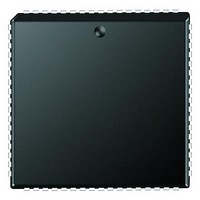
PIC18F6680-I/L Microchip Technology, PIC18F6680-I/L Datasheet - Page 282

PIC18F6680-I/L
Manufacturer Part Number
PIC18F6680-I/L
Description
Microcontrollers (MCU) 64KB 3328 RAM 52 I/O
Manufacturer
Microchip Technology
Datasheet
1.PCM18XK1.pdf
(496 pages)
Specifications of PIC18F6680-I/L
Processor Series
PIC18F
Core
PIC
Data Bus Width
8 bit
Data Ram Size
3.25 KB
Interface Type
I2C/SPI/AUSART/CAN
Maximum Clock Frequency
40 MHz
Number Of Programmable I/os
53
Number Of Timers
5
Operating Supply Voltage
4.2 V to 5.5 V
Maximum Operating Temperature
+ 85 C
Mounting Style
SMD/SMT
3rd Party Development Tools
52715-96, 52716-328, 52717-734, 52712-325, EWPIC18
Development Tools By Supplier
PG164130, DV164035, DV244005, DV164005, PG164120, ICE2000, ICE4000, DV164136
Minimum Operating Temperature
- 40 C
On-chip Adc
12-ch x 10-bit
Program Memory Type
Flash
Program Memory Size
64 KB
Package / Case
PLCC-68
Lead Free Status / RoHS Status
Lead free / RoHS Compliant
Available stocks
Company
Part Number
Manufacturer
Quantity
Price
Company:
Part Number:
PIC18F6680-I/L
Manufacturer:
RUBYCON
Quantity:
46 000
Part Number:
PIC18F6680-I/L
Manufacturer:
MICROCH
Quantity:
20 000
- Current page: 282 of 496
- Download datasheet (9Mb)
PIC18F6585/8585/6680/8680
REGISTER 23-2:
DS30491C-page 280
bit 4-0
CANSTAT: CAN STATUS REGISTER (CONTINUED)
Legend:
C = Clearable bit
‘1’ = Bit is set
Mode 1,2:
EICODE4:EICODE0: Interrupt Code bits in Mode 1 and Mode 2
When an interrupt occurs, a prioritized coded interrupt value will be present in these bits. This
code indicates the source of the interrupt. Unlike ICODE bits in Mode 0, these bits may not be
copied directly to EWIN bits to map interrupted buffer to Access Bank area. If required, user
software may maintain a table in program memory to map EICODE bits to EWIN bits and access
interrupt buffer in Access Bank area.
No interrupt
Error interrupt
TXB2 interrupt
TXB1 interrupt
TXB0 interrupt
RXB1 interrupt
RXB0 interrupt
Wake-up interrupt
RX/TX B0 interrupt
RX/TX B1 interrupt
RX/TX B2 interrupt
RX/TX B3 interrupt
RX/TX B4 interrupt
RX/TX B4 interrupt
Note 1: To achieve maximum power saving and/or able to wake-up on CAN bus activity,
2: In Mode 2, if the buffer is configured as a receiver, EICODE bits will always contain
switch CAN module to Disable mode before putting the device to Sleep.
‘10000’ upon interrupt.
U = Unimplemented bit, read as ‘0’
R = Readable bit
‘0’ = Bit is cleared
EICODE4:EICODE0 Value
10001/10000
10010
10011
10100
10101
10110
10111
00000
00010
00100
00110
01000
10000
01110
(2)
(2)
(2)
(2)
(2)
(2)
W = Writable bit
(2)
- n = Value at POR
x = Bit is unknown
2004 Microchip Technology Inc.
Related parts for PIC18F6680-I/L
Image
Part Number
Description
Manufacturer
Datasheet
Request
R

Part Number:
Description:
20-Pin USB Flash Microcontrollers
Manufacturer:
MICROCHIP [Microchip Technology]
Datasheet:

Part Number:
Description:
PIC18F With 128-segment LCD Driver And 12-bit ADC, 8KB Flash, 768B RAM, CCP, MSS
Manufacturer:
Microchip Technology
Datasheet:

Part Number:
Description:
PIC18F With 128-segment LCD Driver And 12-bit ADC, 16KB Flash, 768B RAM, CCP, MS
Manufacturer:
Microchip Technology
Datasheet:

Part Number:
Description:
PIC18F With 192-segment LCD Driver And 12-bit ADC, 8KB Flash, 768B RAM, CCP, MSS
Manufacturer:
Microchip Technology
Datasheet:

Part Number:
Description:
PIC18F With 192-segment LCD Driver And 12-bit ADC, 16KB Flash, 768B RAM, CCP, MS
Manufacturer:
Microchip Technology
Datasheet:

Part Number:
Description:
Microcontrollers (MCU) 48KB 3328 RAM 52 I/O
Manufacturer:
Microchip Technology
Datasheet:

Part Number:
Description:
32kB Flash, 2kB RAM, 1kB EE, NanoWatt XLP, LCD 64 QFN 9x9x0.9mm T/R
Manufacturer:
Microchip Technology
Datasheet:

Part Number:
Description:
32kB Flash, 2kB RAM, 1kB EE, NanoWatt XLP, LCD 64 TQFP 10x10x1mm T/R
Manufacturer:
Microchip Technology
Datasheet:

Part Number:
Description:
128kB Flash, 4kB RAM, 1kB EE, 16MIPS, NanoWatt XLP, LCD, 5V 80 TQFP 12x12x1mm T/
Manufacturer:
Microchip Technology
Datasheet:

Part Number:
Description:
32kB Flash, 2kB RAM, 1kB EE, NanoWatt XLP, LCD 64 QFN 9x9x0.9mm TUBE
Manufacturer:
Microchip Technology
Datasheet:

Part Number:
Description:
32kB Flash, 2kB RAM, 1kB EE, NanoWatt XLP, LCD 64 TQFP 10x10x1mm TRAY
Manufacturer:
Microchip Technology

Part Number:
Description:
128kB Flash, 4kB RAM, 1kB EE, 16MIPS, NanoWatt XLP, LCD, 5V 80 TQFP 12x12x1mm TR
Manufacturer:
Microchip Technology

Part Number:
Description:
Manufacturer:
Microchip Technology Inc.
Datasheet:


