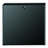
PIC18F6680-I/L Microchip Technology, PIC18F6680-I/L Datasheet - Page 17

PIC18F6680-I/L
Manufacturer Part Number
PIC18F6680-I/L
Description
Microcontrollers (MCU) 64KB 3328 RAM 52 I/O
Manufacturer
Microchip Technology
Datasheet
1.PCM18XK1.pdf
(496 pages)
Specifications of PIC18F6680-I/L
Processor Series
PIC18F
Core
PIC
Data Bus Width
8 bit
Data Ram Size
3.25 KB
Interface Type
I2C/SPI/AUSART/CAN
Maximum Clock Frequency
40 MHz
Number Of Programmable I/os
53
Number Of Timers
5
Operating Supply Voltage
4.2 V to 5.5 V
Maximum Operating Temperature
+ 85 C
Mounting Style
SMD/SMT
3rd Party Development Tools
52715-96, 52716-328, 52717-734, 52712-325, EWPIC18
Development Tools By Supplier
PG164130, DV164035, DV244005, DV164005, PG164120, ICE2000, ICE4000, DV164136
Minimum Operating Temperature
- 40 C
On-chip Adc
12-ch x 10-bit
Program Memory Type
Flash
Program Memory Size
64 KB
Package / Case
PLCC-68
Lead Free Status / RoHS Status
Lead free / RoHS Compliant
Available stocks
Company
Part Number
Manufacturer
Quantity
Price
Company:
Part Number:
PIC18F6680-I/L
Manufacturer:
RUBYCON
Quantity:
46 000
Part Number:
PIC18F6680-I/L
Manufacturer:
MICROCH
Quantity:
20 000
- Current page: 17 of 496
- Download datasheet (9Mb)
TABLE 1-2:
2004 Microchip Technology Inc.
RC0/T1OSO/T13CKI
RC1/T1OSI/CCP2
RC2/CCP1/P1A
RC3/SCK/SCL
RC4/SDI/SDA
RC5/SDO
RC6/TX/CK
RC7/RX/DT
Legend: TTL
Note 1:
RC0
T1OSO
T13CKI
RC1
T1OSI
CCP2
RC2
CCP1
P1A
RC3
SCK
SCL
RC4
SDI
SDA
RC5
SDO
RC6
TX
CK
RC7
RX
DT
2:
3:
4:
5:
6:
7:
Pin Name
(1, 4)
ST
I
P
Alternate assignment for CCP2 in all operating modes except Microcontroller – applies to PIC18F8X8X only.
Default assignment when CCP2MX is set.
External memory interface functions are only available on PIC18F8X8X devices.
CCP2 is multiplexed with this pin by default when configured in Microcontroller mode; otherwise, it is
multiplexed with either RB3 or RC1.
PORTH and PORTJ are only available on PIC18F8X8X (80-pin) devices.
PSP is available in Microcontroller mode only.
On PIC18F8X8X devices, these pins can be multiplexed with RH7/RH6 by changing the ECCPMX
configuration bit.
PIC18F6585/8585/6680/8680 PINOUT I/O DESCRIPTIONS (CONTINUED)
= TTL compatible input
= Schmitt Trigger input with CMOS levels
= Input
= Power
TQFP PLCC
PIC18F6X8X PIC18F8X8X
30
29
33
34
35
36
31
32
Pin Number
41
40
44
45
46
47
42
43
PIC18F6585/8585/6680/8680
TQFP
36
35
43
44
45
46
37
38
Type
Pin
I/O
I/O
I/O
I/O
I/O
I/O
I/O
I/O
I/O
I/O
I/O
I/O
I/O
I/O
I/O
I/O
O
O
O
I
I
I
I
CMOS = CMOS compatible input or output
Analog = Analog input
O
OD
CMOS
Buffer
Type
ST
ST
ST
ST
ST
ST
ST
ST
ST
ST
ST
ST
ST
ST
ST
ST
ST
ST
ST
—
—
—
= Output
= Open-Drain (no P diode to V
PORTC is a bidirectional I/O port.
Digital I/O.
Timer1 oscillator output.
Timer1/Timer3 external clock input.
Digital I/O.
Timer1 oscillator input.
CCP2 Capture input/Compare output/
PWM 2 output.
Digital I/O.
CCP1 Capture input/Compare output.
CCP1 PWM output A.
Digital I/O.
Synchronous serial clock input/output
for SPI mode.
Synchronous serial clock input/output
for I
Digital I/O.
SPI data in.
I
Digital I/O.
SPI data out.
Digital I/O.
USART asynchronous transmit.
USART synchronous clock
(see RX/DT).
Digital I/O.
USART 1 asynchronous receive.
USART 1 synchronous data
(see TX/CK).
2
C data I/O.
2
C mode.
Description
DS30491C-page 15
DD
)
Related parts for PIC18F6680-I/L
Image
Part Number
Description
Manufacturer
Datasheet
Request
R

Part Number:
Description:
20-Pin USB Flash Microcontrollers
Manufacturer:
MICROCHIP [Microchip Technology]
Datasheet:

Part Number:
Description:
PIC18F With 128-segment LCD Driver And 12-bit ADC, 8KB Flash, 768B RAM, CCP, MSS
Manufacturer:
Microchip Technology
Datasheet:

Part Number:
Description:
PIC18F With 128-segment LCD Driver And 12-bit ADC, 16KB Flash, 768B RAM, CCP, MS
Manufacturer:
Microchip Technology
Datasheet:

Part Number:
Description:
PIC18F With 192-segment LCD Driver And 12-bit ADC, 8KB Flash, 768B RAM, CCP, MSS
Manufacturer:
Microchip Technology
Datasheet:

Part Number:
Description:
PIC18F With 192-segment LCD Driver And 12-bit ADC, 16KB Flash, 768B RAM, CCP, MS
Manufacturer:
Microchip Technology
Datasheet:

Part Number:
Description:
Microcontrollers (MCU) 48KB 3328 RAM 52 I/O
Manufacturer:
Microchip Technology
Datasheet:

Part Number:
Description:
32kB Flash, 2kB RAM, 1kB EE, NanoWatt XLP, LCD 64 QFN 9x9x0.9mm T/R
Manufacturer:
Microchip Technology
Datasheet:

Part Number:
Description:
32kB Flash, 2kB RAM, 1kB EE, NanoWatt XLP, LCD 64 TQFP 10x10x1mm T/R
Manufacturer:
Microchip Technology
Datasheet:

Part Number:
Description:
128kB Flash, 4kB RAM, 1kB EE, 16MIPS, NanoWatt XLP, LCD, 5V 80 TQFP 12x12x1mm T/
Manufacturer:
Microchip Technology
Datasheet:

Part Number:
Description:
32kB Flash, 2kB RAM, 1kB EE, NanoWatt XLP, LCD 64 QFN 9x9x0.9mm TUBE
Manufacturer:
Microchip Technology
Datasheet:

Part Number:
Description:
32kB Flash, 2kB RAM, 1kB EE, NanoWatt XLP, LCD 64 TQFP 10x10x1mm TRAY
Manufacturer:
Microchip Technology

Part Number:
Description:
128kB Flash, 4kB RAM, 1kB EE, 16MIPS, NanoWatt XLP, LCD, 5V 80 TQFP 12x12x1mm TR
Manufacturer:
Microchip Technology

Part Number:
Description:
Manufacturer:
Microchip Technology Inc.
Datasheet:


