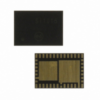
SI1000-C-GM Silicon Laboratories Inc, SI1000-C-GM Datasheet - Page 230

SI1000-C-GM
Manufacturer Part Number
SI1000-C-GM
Description
IC TXRX MCU + EZRADIOPRO
Manufacturer
Silicon Laboratories Inc
Specifications of SI1000-C-GM
Package / Case
42-QFN
Frequency
240MHz ~ 960MHz
Data Rate - Maximum
256kbps
Modulation Or Protocol
FSK, GFSK, OOK
Applications
General Purpose
Power - Output
20dBm
Sensitivity
-121dBm
Voltage - Supply
1.8 V ~ 3.6 V
Current - Receiving
18.5mA
Current - Transmitting
85mA
Data Interface
PCB, Surface Mount
Memory Size
64kB Flash, 4kB RAM
Antenna Connector
PCB, Surface Mount
Number Of Receivers
1
Number Of Transmitters
1
Wireless Frequency
240 MHz to 960 MHz
Interface Type
UART, SMBus, SPI, PCA
Output Power
20 dBm
Operating Supply Voltage
0.9 V to 3.6 V
Maximum Operating Temperature
+ 85 C
Mounting Style
SMD/SMT
Maximum Supply Current
4.1 mA
Minimum Operating Temperature
- 40 C
Modulation
FSK, GFSK, OOK
Protocol Supported
C2, SMBus
Core
8051
Program Memory Type
Flash
Program Memory Size
64 KB
Data Ram Size
4352 B
Supply Current (max)
4.1 mA
Cpu Family
Si100x
Device Core
8051
Device Core Size
8b
Frequency (max)
25MHz
Total Internal Ram Size
4.25KB
# I/os (max)
22
Number Of Timers - General Purpose
4
Operating Supply Voltage (typ)
2.5/3.3V
Operating Supply Voltage (max)
3.6V
Operating Supply Voltage (min)
1.8V
On-chip Adc
18-chx10-bit
Instruction Set Architecture
CISC
Mounting
Surface Mount
Pin Count
42
Package Type
QFN EP
Lead Free Status / RoHS Status
Lead free / RoHS Compliant
Operating Temperature
-
Lead Free Status / Rohs Status
Lead free / RoHS Compliant
Other names
336-1881-5
Available stocks
Company
Part Number
Manufacturer
Quantity
Price
Company:
Part Number:
SI1000-C-GM
Manufacturer:
FSC
Quantity:
1 000
- Current page: 230 of 376
- Download datasheet (3Mb)
Si1000/1/2/3/4/5
To read back data from the transceiver, the R/W bit must be set to 0 followed by the 7-bit address of the
register from which to read. The 8 bit DATA field following the 7-bit ADDR field is ignored on the MOSI pin
when R/W = 0. The next eight negative edge transitions of the SCK signal will clock out the contents of the
selected register. The data read from the selected register will be available on the MISO output. The READ
function is shown in Figure 22.3. After the READ function is completed the MISO signal will remain at
either a logic 1 or logic 0 state depending on the last data bit clocked out (D0). When NSS goes high the
MISO output pin will be pulled high by internal pullup.
230
Symbol
t
t
t
t
t
t
t
t
t
t
SW
CH
DS
DH
DD
EN
DE
SS
SH
CL
SCLK
NSS
MOSI
nSEL
SDI
SDO
MOSI
SCL
MISO
NSS
Output disable time
SCLK
nSEL
Output enable time
SDI
Select high period
Output data delay
Select setup time
Select hold time
Data setup time
Clock high time
Clock low time
Data hold time
Parameter
MSB
time
MSB
First Bit
RW
RW
=0
A6 A5
Table 22.1. Serial Interface Timing Parameters
A6
A5
Address
Figure 22.3. SPI Timing—READ Mode
A4
A4
(nsec)
A3
Min
40
40
20
20
20
20
50
20
50
80
A3
Figure 22.2. SPI Timing
A2 A1 A0 D7 D6 D5 D4 D3 D2 D1 D0
A2
A1
SCL
MOSI
MISO
NSS
SDI
SCLK
SDO
nSEL
First Bit
A0
Rev. 1.0
D7
D7
=X
t
t
EN
SS
D6 D5 D4 D3
D6
=X
D5
=X
Data
t
CL
D4
=X
t
D3
=X
CH
Diagram
D2
=X
D2 D1 D0
t
DS
D1
=X
t
DH
Last Bit
D0
=X
Last Bit
LSB
t
DD
xx xx
t
SH
RW A7
t
DE
t
SW
Related parts for SI1000-C-GM
Image
Part Number
Description
Manufacturer
Datasheet
Request
R
Part Number:
Description:
QFN 42/I�/915 MHZ, SNAP ENABLED PROGRAMABLE XCVR
Manufacturer:
Silicon Laboratories Inc
Part Number:
Description:
QFN 42/I�/64KB, 4KB RAM, +20 DBM, PROGRAMMABLE XCVR
Manufacturer:
Silicon Laboratories Inc
Part Number:
Description:
Microcontrollers (MCU) 915MHz SNAP enabled program XCVR
Manufacturer:
Silicon Laboratories Inc
Datasheet:

Part Number:
Description:
BOARD EVALUATION FOR SI1000
Manufacturer:
Silicon Laboratories Inc
Datasheet:

Part Number:
Description:
BOARD EVALUATION FOR SI1000
Manufacturer:
Silicon Laboratories Inc
Datasheet:

Part Number:
Description:
BOARD EVALUATION FOR SI1012
Manufacturer:
Silicon Laboratories Inc
Datasheet:

Part Number:
Description:
BOARD EVALUATION FOR SI1002
Manufacturer:
Silicon Laboratories Inc
Datasheet:

Part Number:
Description:
DEVELOPMENT KIT SI101X
Manufacturer:
Silicon Laboratories Inc
Datasheet:

Part Number:
Description:
BOARD EVALUATION FOR SI1004
Manufacturer:
Silicon Laboratories Inc
Datasheet:

Part Number:
Description:
BOARD EVALUATION FOR SI1004
Manufacturer:
Silicon Laboratories Inc
Datasheet:

Part Number:
Description:
BOARD EVALUATION FOR SI1012
Manufacturer:
Silicon Laboratories Inc
Datasheet:

Part Number:
Description:
BOARD EVALUATION FOR SI1014
Manufacturer:
Silicon Laboratories Inc
Datasheet:

Part Number:
Description:
DEVELOPMENT KIT SI101X
Manufacturer:
Silicon Laboratories Inc
Datasheet:


