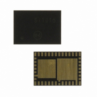
SI1000-C-GM Silicon Laboratories Inc, SI1000-C-GM Datasheet - Page 147

SI1000-C-GM
Manufacturer Part Number
SI1000-C-GM
Description
IC TXRX MCU + EZRADIOPRO
Manufacturer
Silicon Laboratories Inc
Specifications of SI1000-C-GM
Package / Case
42-QFN
Frequency
240MHz ~ 960MHz
Data Rate - Maximum
256kbps
Modulation Or Protocol
FSK, GFSK, OOK
Applications
General Purpose
Power - Output
20dBm
Sensitivity
-121dBm
Voltage - Supply
1.8 V ~ 3.6 V
Current - Receiving
18.5mA
Current - Transmitting
85mA
Data Interface
PCB, Surface Mount
Memory Size
64kB Flash, 4kB RAM
Antenna Connector
PCB, Surface Mount
Number Of Receivers
1
Number Of Transmitters
1
Wireless Frequency
240 MHz to 960 MHz
Interface Type
UART, SMBus, SPI, PCA
Output Power
20 dBm
Operating Supply Voltage
0.9 V to 3.6 V
Maximum Operating Temperature
+ 85 C
Mounting Style
SMD/SMT
Maximum Supply Current
4.1 mA
Minimum Operating Temperature
- 40 C
Modulation
FSK, GFSK, OOK
Protocol Supported
C2, SMBus
Core
8051
Program Memory Type
Flash
Program Memory Size
64 KB
Data Ram Size
4352 B
Supply Current (max)
4.1 mA
Cpu Family
Si100x
Device Core
8051
Device Core Size
8b
Frequency (max)
25MHz
Total Internal Ram Size
4.25KB
# I/os (max)
22
Number Of Timers - General Purpose
4
Operating Supply Voltage (typ)
2.5/3.3V
Operating Supply Voltage (max)
3.6V
Operating Supply Voltage (min)
1.8V
On-chip Adc
18-chx10-bit
Instruction Set Architecture
CISC
Mounting
Surface Mount
Pin Count
42
Package Type
QFN EP
Lead Free Status / RoHS Status
Lead free / RoHS Compliant
Operating Temperature
-
Lead Free Status / Rohs Status
Lead free / RoHS Compliant
Other names
336-1881-5
Available stocks
Company
Part Number
Manufacturer
Quantity
Price
Company:
Part Number:
SI1000-C-GM
Manufacturer:
FSC
Quantity:
1 000
- Current page: 147 of 376
- Download datasheet (3Mb)
13.6. Minimizing Flash Read Current
The Flash memory in the Si1000/1/2/3/4/5 devices is responsible for a substantial portion of the total digital
supply current when the device is executing code. Below are suggestions to minimize Flash read current.
1. Use Idle, Suspend, or Sleep Modes while waiting for an interrupt, rather than polling the interrupt flag.
2. Si1000/1/2/3/4/5 devices have a one-shot timer that saves power when operating at system clock
3. Flash read current depends on the number of address lines that toggle between sequential Flash read
4. The Flash memory is organized in rows. Each row in the Si1000/1/2/3/4/5 Flash contains 128 bytes. A
5. To minimize the power consumption of small loops, it is best to locate them within a single row, if
Note: Future 16 and 8 kB derivatives in this product family will use a Flash memory that is organized in rows of 64
Idle Mode is particularly well-suited for use in implementing short pauses, since the wake-up time is no
more than three system clock cycles. See the Power Management chapter for details on the various
low-power operating modes.
frequencies of 10 MHz or less. The one-shot timer generates a minimum-duration enable signal for the
Flash sense amps on each clock cycle in which the Flash memory is accessed. This allows the Flash to
remain in a low power state for the remainder of the long clock cycle.
At clock frequencies above 10 MHz, the system clock cycle becomes short enough that the one-shot
timer no longer provides a power benefit. Disabling the one-shot timer at higher frequencies reduces
power consumption. The one-shot is enabled by default, and it can be disabled (bypassed) by setting
the BYPASS bit (FLSCL.6) to logic 1. To re-enable the one-shot, clear the BYPASS bit to logic 0. See
the note in SFR Definition 13.3. FLSCL: Flash Scale for more information on how to properly clear the
BYPASS bit.
operations. In most cases, the difference in power is relatively small (on the order of 5%).
substantial current increase can be detected when the read address jumps from one row in the Flash
memory to another. Consider a 3-cycle loop (e.g., SJMP $, or while(1);) which straddles a 128-byte
Flash row boundary. The Flash address jumps from one row to another on two of every three clock
cycles. This can result in a current increase of up 30% when compared to the same 3-cycle loop
contained entirely within a single row.
possible. To check if a loop is contained within a Flash row, divide the starting address of the first
instruction in the loop by 128. If the remainder (result of modulo operation) plus the length of the loop is
less than 127, then the loop fits inside a single Flash row. Otherwise, the loop will be straddling two
adjacent Flash rows. If a loop executes in 20 or more clock cycles, then the transitions from one row to
another will occur on relatively few clock cycles, and any resulting increase in operating current will be
negligible.
bytes each. To maintain code compatibility across the entire family, it is best to locate small loops within a single
64-byte segment.
Rev. 1.0
Si1000/1/2/3/4/5
147
Related parts for SI1000-C-GM
Image
Part Number
Description
Manufacturer
Datasheet
Request
R
Part Number:
Description:
QFN 42/I�/915 MHZ, SNAP ENABLED PROGRAMABLE XCVR
Manufacturer:
Silicon Laboratories Inc
Part Number:
Description:
QFN 42/I�/64KB, 4KB RAM, +20 DBM, PROGRAMMABLE XCVR
Manufacturer:
Silicon Laboratories Inc
Part Number:
Description:
Microcontrollers (MCU) 915MHz SNAP enabled program XCVR
Manufacturer:
Silicon Laboratories Inc
Datasheet:

Part Number:
Description:
BOARD EVALUATION FOR SI1000
Manufacturer:
Silicon Laboratories Inc
Datasheet:

Part Number:
Description:
BOARD EVALUATION FOR SI1000
Manufacturer:
Silicon Laboratories Inc
Datasheet:

Part Number:
Description:
BOARD EVALUATION FOR SI1012
Manufacturer:
Silicon Laboratories Inc
Datasheet:

Part Number:
Description:
BOARD EVALUATION FOR SI1002
Manufacturer:
Silicon Laboratories Inc
Datasheet:

Part Number:
Description:
DEVELOPMENT KIT SI101X
Manufacturer:
Silicon Laboratories Inc
Datasheet:

Part Number:
Description:
BOARD EVALUATION FOR SI1004
Manufacturer:
Silicon Laboratories Inc
Datasheet:

Part Number:
Description:
BOARD EVALUATION FOR SI1004
Manufacturer:
Silicon Laboratories Inc
Datasheet:

Part Number:
Description:
BOARD EVALUATION FOR SI1012
Manufacturer:
Silicon Laboratories Inc
Datasheet:

Part Number:
Description:
BOARD EVALUATION FOR SI1014
Manufacturer:
Silicon Laboratories Inc
Datasheet:

Part Number:
Description:
DEVELOPMENT KIT SI101X
Manufacturer:
Silicon Laboratories Inc
Datasheet:


