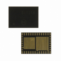
SI1000-C-GM Silicon Laboratories Inc, SI1000-C-GM Datasheet - Page 168

SI1000-C-GM
Manufacturer Part Number
SI1000-C-GM
Description
IC TXRX MCU + EZRADIOPRO
Manufacturer
Silicon Laboratories Inc
Specifications of SI1000-C-GM
Package / Case
42-QFN
Frequency
240MHz ~ 960MHz
Data Rate - Maximum
256kbps
Modulation Or Protocol
FSK, GFSK, OOK
Applications
General Purpose
Power - Output
20dBm
Sensitivity
-121dBm
Voltage - Supply
1.8 V ~ 3.6 V
Current - Receiving
18.5mA
Current - Transmitting
85mA
Data Interface
PCB, Surface Mount
Memory Size
64kB Flash, 4kB RAM
Antenna Connector
PCB, Surface Mount
Number Of Receivers
1
Number Of Transmitters
1
Wireless Frequency
240 MHz to 960 MHz
Interface Type
UART, SMBus, SPI, PCA
Output Power
20 dBm
Operating Supply Voltage
0.9 V to 3.6 V
Maximum Operating Temperature
+ 85 C
Mounting Style
SMD/SMT
Maximum Supply Current
4.1 mA
Minimum Operating Temperature
- 40 C
Modulation
FSK, GFSK, OOK
Protocol Supported
C2, SMBus
Core
8051
Program Memory Type
Flash
Program Memory Size
64 KB
Data Ram Size
4352 B
Supply Current (max)
4.1 mA
Cpu Family
Si100x
Device Core
8051
Device Core Size
8b
Frequency (max)
25MHz
Total Internal Ram Size
4.25KB
# I/os (max)
22
Number Of Timers - General Purpose
4
Operating Supply Voltage (typ)
2.5/3.3V
Operating Supply Voltage (max)
3.6V
Operating Supply Voltage (min)
1.8V
On-chip Adc
18-chx10-bit
Instruction Set Architecture
CISC
Mounting
Surface Mount
Pin Count
42
Package Type
QFN EP
Lead Free Status / RoHS Status
Lead free / RoHS Compliant
Operating Temperature
-
Lead Free Status / Rohs Status
Lead free / RoHS Compliant
Other names
336-1881-5
Available stocks
Company
Part Number
Manufacturer
Quantity
Price
Company:
Part Number:
SI1000-C-GM
Manufacturer:
FSC
Quantity:
1 000
- Current page: 168 of 376
- Download datasheet (3Mb)
Si1000/1/2/3/4/5
When the dc-dc converter “Enabled” configuration (one-cell mode) is chosen, the following guidelines
apply:
16.5. Minimizing Power Supply Noise
To minimize noise on the power supply lines, the GND/VBAT- and GND_MCU/DC- pins should be kept
separate, as shown in Figure 16.2; GND_MCU/DC- should be connected to the pc board ground plane.
The large decoupling capacitors in the input and output circuits ensure that each supply is relatively quiet
with respect to its own ground. However, connecting a circuit element "diagonally" (e.g., connecting an
external chip between VDD_MCU/DC+ and GND/VBAT-, or between VBAT and GND_MCU/DC-) can
result in high supply noise across that circuit element.
To accommodate situations in which ADC0 is sampling a signal that is referenced to one of the external
grounds, we recommend using the Analog Ground Reference (P0.1/AGND) option described in Section
5.12. This option prevents any voltage differences between the internal chip ground and the external
grounds from modulating the ADC input signal. If this option is enabled, the P0.1 pin should be tied to the
168
DC-DC Converter
Enabled
0.9 to 1.8 V
Supply Voltage
(one-cell mode)
DC-DC Converter
Disabled
1.8 to 3.6 V
Supply Voltage
(two-cell mode)
In most cases, the GND/VBAT– pin should not be externally connected to GND.
The 0.68 µH inductor should be placed as close as possible to the DCEN pin for maximum efficiency.
The 4.7 µF capacitor should be placed as close as possible to the inductor.
The current loop including GND/VBAT-, the 4.7 µF capacitor, the 0.68 µH inductor and the DCEN pin
should be made as short as possible to minimize capacitance.
The PCB traces connecting VDD_MCU/DC+ to the output capacitor and the output capacitor to
GND_MCU/DC– should be as short and as thick as possible in order to minimize parasitic inductance.
Figure 16.2. DC-DC Converter Configuration Options
VBAT
VBAT
Rev. 1.0
4.7 uF
GND/VBAT-
GND/VBAT-
0.68 uH
DCEN
DCEN
VDD_MCU/
VDD_MCU/
DC+
DC+
GND_MCU/
GND_MCU/
DC-
DC-
1 uF
Related parts for SI1000-C-GM
Image
Part Number
Description
Manufacturer
Datasheet
Request
R
Part Number:
Description:
QFN 42/I�/915 MHZ, SNAP ENABLED PROGRAMABLE XCVR
Manufacturer:
Silicon Laboratories Inc
Part Number:
Description:
QFN 42/I�/64KB, 4KB RAM, +20 DBM, PROGRAMMABLE XCVR
Manufacturer:
Silicon Laboratories Inc
Part Number:
Description:
Microcontrollers (MCU) 915MHz SNAP enabled program XCVR
Manufacturer:
Silicon Laboratories Inc
Datasheet:

Part Number:
Description:
BOARD EVALUATION FOR SI1000
Manufacturer:
Silicon Laboratories Inc
Datasheet:

Part Number:
Description:
BOARD EVALUATION FOR SI1000
Manufacturer:
Silicon Laboratories Inc
Datasheet:

Part Number:
Description:
BOARD EVALUATION FOR SI1012
Manufacturer:
Silicon Laboratories Inc
Datasheet:

Part Number:
Description:
BOARD EVALUATION FOR SI1002
Manufacturer:
Silicon Laboratories Inc
Datasheet:

Part Number:
Description:
DEVELOPMENT KIT SI101X
Manufacturer:
Silicon Laboratories Inc
Datasheet:

Part Number:
Description:
BOARD EVALUATION FOR SI1004
Manufacturer:
Silicon Laboratories Inc
Datasheet:

Part Number:
Description:
BOARD EVALUATION FOR SI1004
Manufacturer:
Silicon Laboratories Inc
Datasheet:

Part Number:
Description:
BOARD EVALUATION FOR SI1012
Manufacturer:
Silicon Laboratories Inc
Datasheet:

Part Number:
Description:
BOARD EVALUATION FOR SI1014
Manufacturer:
Silicon Laboratories Inc
Datasheet:

Part Number:
Description:
DEVELOPMENT KIT SI101X
Manufacturer:
Silicon Laboratories Inc
Datasheet:


