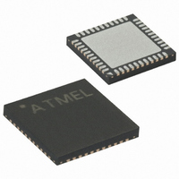
ATMEGA64RZAV-10MU Atmel, ATMEGA64RZAV-10MU Datasheet - Page 12

ATMEGA64RZAV-10MU
Manufacturer Part Number
ATMEGA64RZAV-10MU
Description
MCU ATMEGA644/AT86RF230 44-QFN
Manufacturer
Atmel
Series
ATMEGAr
Datasheets
1.ATMEGA644-20MU.pdf
(23 pages)
2.ATMEGA644-20MU.pdf
(376 pages)
3.AT86RF230-ZU.pdf
(98 pages)
Specifications of ATMEGA64RZAV-10MU
Frequency
2.4GHz
Modulation Or Protocol
802.15.4 Zigbee
Power - Output
3dBm
Sensitivity
-101dBm
Voltage - Supply
1.8 V ~ 3.6 V
Data Interface
PCB, Surface Mount
Memory Size
64kB Flash, 2kB EEPROM, 4kB RAM
Antenna Connector
PCB, Surface Mount
Package / Case
44-VFQFN Exposed Pad
Wireless Frequency
2.4 GHz
Interface Type
JTAG, SPI
Output Power
3 dBm
For Use With
ATSTK600-TQFP32 - STK600 SOCKET/ADAPTER 32-TQFP770-1005 - ISP 4PORT FOR ATMEL AVR MCU JTAG770-1004 - ISP 4PORT FOR ATMEL AVR MCU SPIATAVRISP2 - PROGRAMMER AVR IN SYSTEMATJTAGICE2 - AVR ON-CHIP D-BUG SYSTEMATSTK500 - PROGRAMMER AVR STARTER KIT
Lead Free Status / RoHS Status
Lead free / RoHS Compliant
Operating Temperature
-
Applications
-
Data Rate - Maximum
-
Current - Transmitting
-
Current - Receiving
-
Lead Free Status / Rohs Status
Lead free / RoHS Compliant
For Use With/related Products
ATmega64
6.2 SPI Protocol
Table 6-2. SPI Command Byte Definition
6.2.1 Register Access Mode
12
Bit 7
1
1
0
0
0
0
AT86RF230
Bit 6
0
1
0
1
0
1
Bit 5
1
1
0
0
Bit 4
master device or an external pull-up resistor. Note, when both SEL and RST are
active, the MISO output driver is also enabled.
The MOSI line is sampled by the radio transceiver at the rising edge of SCLK. The
signal must be stable before and after the rising edge of SCLK as specified by t
refer to section 11.4 parameters 11.4.5 and 11.4.6.
This mode of SPI operation is commonly called “SPI Mode 0”.
Each transfer sequence starts with transferring a command byte from SPI master via
MOSI (see Table 6-2) with MSB first. This command byte defines the access mode and
additional mode-dependent information.
The different access modes are described within the following sections.
In Figure 6-4 to Figure 6-14 logic values stated with X on MOSI are ignored by the radio
transceiver, but need to have a valid level. Return values on MISO stated as X shall be
ignored by the microcontroller.
The Register access mode is a two-byte read/write operation and is initiated by setting
register access (see Table 6-2) and a register address (see Table 12-1).
On write access the second byte transferred on MOSI contains the write data to the
selected address (see Figure 6-4).
Figure 6-4. Packet Structure – Register Write Access
On read access the content of the selected register address is returned in the second
byte on MISO (see Figure 6-5).
SEL = L. The first transferred byte on MOSI is the command byte and must indicate a
MOSI
MISO
Register address [5:0]
Register address [5:0]
Bit 3
1
byte 1 (command byte)
1
Reserved
Reserved
Reserved
Reserved
Bit 2
address[5:0]
XX
Bit 1
Bit 0
write data[7:0]
byte 2 (data byte)
XX
Mode
Register Access Mode – Read Access
Register Access Mode – Write Access
Frame Buffer Access Mode – Read Access
Frame Buffer Access Mode – Write Access
SRAM Access Mode – Read Access
SRAM Access Mode – Write Access
5131E-MCU Wireless-02/09
3
and t
4
,


