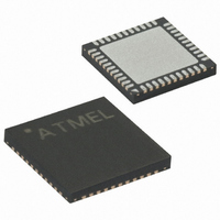
ATMEGA64RZAV-10MU Atmel, ATMEGA64RZAV-10MU Datasheet - Page 11

ATMEGA64RZAV-10MU
Manufacturer Part Number
ATMEGA64RZAV-10MU
Description
MCU ATMEGA644/AT86RF230 44-QFN
Manufacturer
Atmel
Series
ATMEGAr
Datasheets
1.ATMEGA644-20MU.pdf
(23 pages)
2.ATMEGA644-20MU.pdf
(376 pages)
3.AT86RF230-ZU.pdf
(98 pages)
Specifications of ATMEGA64RZAV-10MU
Frequency
2.4GHz
Modulation Or Protocol
802.15.4 Zigbee
Power - Output
3dBm
Sensitivity
-101dBm
Voltage - Supply
1.8 V ~ 3.6 V
Data Interface
PCB, Surface Mount
Memory Size
64kB Flash, 2kB EEPROM, 4kB RAM
Antenna Connector
PCB, Surface Mount
Package / Case
44-VFQFN Exposed Pad
Wireless Frequency
2.4 GHz
Interface Type
JTAG, SPI
Output Power
3 dBm
For Use With
ATSTK600-TQFP32 - STK600 SOCKET/ADAPTER 32-TQFP770-1005 - ISP 4PORT FOR ATMEL AVR MCU JTAG770-1004 - ISP 4PORT FOR ATMEL AVR MCU SPIATAVRISP2 - PROGRAMMER AVR IN SYSTEMATJTAGICE2 - AVR ON-CHIP D-BUG SYSTEMATSTK500 - PROGRAMMER AVR STARTER KIT
Lead Free Status / RoHS Status
Lead free / RoHS Compliant
Operating Temperature
-
Applications
-
Data Rate - Maximum
-
Current - Transmitting
-
Current - Receiving
-
Lead Free Status / Rohs Status
Lead free / RoHS Compliant
For Use With/related Products
ATmega64
6.1 SPI Timing Description
Figure 6-2. SPI Timing, Global Map and Definition of Timing Parameters t
Figure 6-3. SPI Timing, Detailed View and Definition of Timing Parameters t
SCLK
MOSI
MISO
5131E-MCU Wireless-02/09
SEL
t
0
t
1
t
3
Bit 7
t
4
Bit 7
The SPI is designed to work in synchronous or asynchronous mode.
In synchronous mode, the CLKM output of the radio transceiver is used as the master
clock of the microcontroller. In this case the maximum SPI clock frequency is 8 MHz.
In asynchronous mode, the SPI master clock (SCLK) is generated by the
microcontroller itself. The maximum SPI clock rate is limited to 7.5 MHz using this
operating mode. If the clock signal from the radio transceiver pin CLKM is not required,
it may be disabled.
Figure 6-2 and Figure 6-3 illustrate the SPI timing and introduce its parameters. The
corresponding timing parameter definition is given in Table 11-4.
The SPI is based on a byte-oriented protocol and is always a bidirectional
communication between master and slave. The SPI master starts the transfer by
asserting SEL = L. Then the master generates eight SPI clock cycles to transfer a byte
to the radio transceiver (via MOSI). At the same time the slave transmits one byte to the
master (via MISO). When the master wants to receive one byte of data from the slave it
must also transmit one byte to the slave. All bytes are transferred MSB first. An SPI
transaction is finished by releasing SEL = H.
A SPI register access consists of two bytes, a Frame Buffer or SRAM access of two or
more bytes, as described in section 6.2.
valid after t
SCLK. If the MISO output driver is disabled, there is no internal pull-up resistor
connected to the output. Driving the appropriate signal level must be ensured by the
SEL = L enables the MISO output driver of the radio transceiver. The MSB of MISO is
t
2
1
(see section 11.4 parameter 11.4.3) and is updated at each falling edge of
Bit 6
Bit 6
5
, t
0
6
, t
to t
8
and t
4
9
Bit 5
Bit 5
AT86RF230
11


