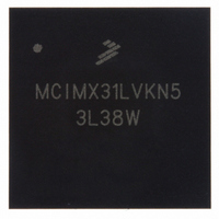
MCIMX31LVKN5 Freescale Semiconductor, MCIMX31LVKN5 Datasheet - Page 58

MCIMX31LVKN5
Manufacturer Part Number
MCIMX31LVKN5
Description
IC MPU MAP I.MX31L 457-MAPBGA
Manufacturer
Freescale Semiconductor
Series
i.MX31r
Datasheet
1.MCIMX31LITEKITC.pdf
(122 pages)
Specifications of MCIMX31LVKN5
Core Processor
ARM11
Core Size
32-Bit
Speed
532MHz
Connectivity
1-Wire, ATA, EBI/EMI, FIR, I²C, MMC/SD, PCMCIA, SIM, SPI, SSI, UART/USART, USB, USB OTG
Peripherals
DMA, LCD, POR, PWM, WDT
Program Memory Type
ROMless
Ram Size
16K x 8
Voltage - Supply (vcc/vdd)
1.22 V ~ 3.3 V
Oscillator Type
External
Operating Temperature
0°C ~ 70°C
Package / Case
457-MAPBGA
Lead Free Status / RoHS Status
Lead free / RoHS Compliant
Number Of I /o
-
Eeprom Size
-
Program Memory Size
-
Data Converters
-
Available stocks
Company
Part Number
Manufacturer
Quantity
Price
Company:
Part Number:
MCIMX31LVKN5
Manufacturer:
ADI
Quantity:
9 710
Company:
Part Number:
MCIMX31LVKN5
Manufacturer:
Freescale Semiconductor
Quantity:
10 000
Company:
Part Number:
MCIMX31LVKN5B
Manufacturer:
Freescale Semiconductor
Quantity:
10 000
Company:
Part Number:
MCIMX31LVKN5BR2
Manufacturer:
Freescale Semiconductor
Quantity:
10 000
Company:
Part Number:
MCIMX31LVKN5C
Manufacturer:
FREESCALE
Quantity:
1 831
Company:
Part Number:
MCIMX31LVKN5C
Manufacturer:
FREESCALE
Quantity:
748
Company:
Part Number:
MCIMX31LVKN5C
Manufacturer:
Freescale Semiconductor
Quantity:
10 000
Part Number:
MCIMX31LVKN5C
Manufacturer:
FREESCALE
Quantity:
20 000
Company:
Part Number:
MCIMX31LVKN5R2
Manufacturer:
IBM
Quantity:
284
Part Number:
MCIMX31LVKN5R2
Manufacturer:
FREESCALE
Quantity:
20 000
Electrical Characteristics
4.3.14.2.2
The SENSB_VSYNC, SENSB_HSYNC, and SENSB_PIX_CLK signals are used in this mode. See
Figure
A frame starts with a rising edge on SENSB_VSYNC (all the timings correspond to straight polarity of the
corresponding signals). Then SENSB_HSYNC goes to high and hold for the entire line. Pixel clock is valid
as long as SENSB_HSYNC is high. Data is latched at the rising edge of the valid pixel clocks.
SENSB_HSYNC goes to low at the end of line. Pixel clocks then become invalid and the CSI stops
receiving data from the stream. For next line the SENSB_HSYNC timing repeats. For next frame the
SENSB_VSYNC timing repeats.
4.3.14.2.3
The timing is the same as the gated-clock mode (described in
except for the SENSB_HSYNC signal, which is not used. See
valid and will cause data to be latched into the input FIFO. The SENSB_PIX_CLK signal is inactive (states
low) until valid data is going to be transmitted over the bus.
58
43.
SENSB_DATA[9:0]
SENSB_PIX_CLK
SENSB_DATA[7:0]
SENSB_HSYNC
SENSB_VSYNC
SENSB_PIX_CLK
SENSB_VSYNC
Gated Clock Mode
Non-Gated Clock Mode
Start of Frame
Start of Frame
invalid
invalid
Figure 44. Non-Gated Clock Mode Timing Diagram
nth frame
nth frame
Figure 43. Gated Clock Mode Timing Diagram
MCIMX31/MCIMX31L Technical Data, Rev. 4.1
1st byte
1st byte
Active Line
n+1th frame
invalid
n+1th frame
Section 4.3.14.2.2, “Gated Clock
invalid
Figure
44. All incoming pixel clocks are
1st byte
1st byte
Freescale Semiconductor
Mode”),


