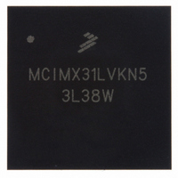
MCIMX31LVKN5 Freescale Semiconductor, MCIMX31LVKN5 Datasheet - Page 112

MCIMX31LVKN5
Manufacturer Part Number
MCIMX31LVKN5
Description
IC MPU MAP I.MX31L 457-MAPBGA
Manufacturer
Freescale Semiconductor
Series
i.MX31r
Datasheet
1.MCIMX31LITEKITC.pdf
(122 pages)
Specifications of MCIMX31LVKN5
Core Processor
ARM11
Core Size
32-Bit
Speed
532MHz
Connectivity
1-Wire, ATA, EBI/EMI, FIR, I²C, MMC/SD, PCMCIA, SIM, SPI, SSI, UART/USART, USB, USB OTG
Peripherals
DMA, LCD, POR, PWM, WDT
Program Memory Type
ROMless
Ram Size
16K x 8
Voltage - Supply (vcc/vdd)
1.22 V ~ 3.3 V
Oscillator Type
External
Operating Temperature
0°C ~ 70°C
Package / Case
457-MAPBGA
Lead Free Status / RoHS Status
Lead free / RoHS Compliant
Number Of I /o
-
Eeprom Size
-
Program Memory Size
-
Data Converters
-
Available stocks
Company
Part Number
Manufacturer
Quantity
Price
Company:
Part Number:
MCIMX31LVKN5
Manufacturer:
ADI
Quantity:
9 710
Company:
Part Number:
MCIMX31LVKN5
Manufacturer:
Freescale Semiconductor
Quantity:
10 000
Company:
Part Number:
MCIMX31LVKN5B
Manufacturer:
Freescale Semiconductor
Quantity:
10 000
Company:
Part Number:
MCIMX31LVKN5BR2
Manufacturer:
Freescale Semiconductor
Quantity:
10 000
Company:
Part Number:
MCIMX31LVKN5C
Manufacturer:
FREESCALE
Quantity:
1 831
Company:
Part Number:
MCIMX31LVKN5C
Manufacturer:
FREESCALE
Quantity:
748
Company:
Part Number:
MCIMX31LVKN5C
Manufacturer:
Freescale Semiconductor
Quantity:
10 000
Part Number:
MCIMX31LVKN5C
Manufacturer:
FREESCALE
Quantity:
20 000
Company:
Part Number:
MCIMX31LVKN5R2
Manufacturer:
IBM
Quantity:
284
Part Number:
MCIMX31LVKN5R2
Manufacturer:
FREESCALE
Quantity:
20 000
Package Information and Pinout
5.2.2
See
5.2.3
Table 67
shows the no-connects.
5.2.3.1
112
GND/PWR ID
FGND
FUSE_VDD
FVCC
GND
IOQVDD
MGND
MVCC
NVCC1
NVCC2
NVCC3
NVCC4
NVCC5
NVCC6
NVCC7
NVCC8
NVCC9
NVCC10
NVCC21
NVCC22
QVCC
QVCC1
QVCC4
SGND
SVCC
UVCC
UGND
Table 71
shows the device connection list for power and ground, alpha-sorted followed by
MAPBGA Signal Assignment–19 × 19 mm 0.8 mm
Connection Tables–
U16
T15
T16
A1, A2, A3, A21, A22, A23, B1, B2, B22, B23, C1, C2, C22, C23, D22, D23, J12, J13, K10, K11, K12, K13, K14,
L10, L11, L12, L13, L14, M9, M10, M11, M12, M13, M14, N10, N11, N12, N13, N14, P10, P11, P12, P13, P14,
R12, Y1, Y23, AA1, AA2, AA22, AA23, AB1, AB2, AB21, AB22, AB23, AC1, AC2, AC21, AC22, AC23
T8
U14
U15
G15, G16, H16, J17
N16, P16, R15, R16, T14
K7, K8, L7, L8
H14, J15, K15
G9, G10, H8, H9
G11, G12, G13, H12
H15, J16, K16, L16, M16
H10, H11, J11
G14
P8, R7, R8, R9, T9
T11, T12, T13, U11
T10, U7, U8, U9, U10, V6, V7, V8, V9, V10
H13, J14, L15, M15, N9, N15, P9, P15, R10, R11, R13, R14
J8, J9, J10, K9
L9, M7, M8, N8
U13
U12
P18
P17
Ground and Power ID Locations—
for the 19
Table 67. 19 x 19 BGA Ground/Power ID by Ball Grid Location
×
Table 69
19 mm, 0.8 mm pitch signal assignments/ball map.
MCIMX31/MCIMX31L Technical Data, Rev. 4.1
shows the device connection list for signals.
19 x 19 mm 0.8 mm
Ball Location
19 x 19 mm 0.8 mm
Freescale Semiconductor
Table
68, which


