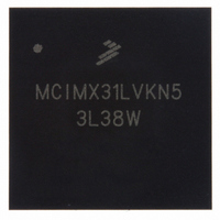
MCIMX31LVKN5 Freescale Semiconductor, MCIMX31LVKN5 Datasheet - Page 22

MCIMX31LVKN5
Manufacturer Part Number
MCIMX31LVKN5
Description
IC MPU MAP I.MX31L 457-MAPBGA
Manufacturer
Freescale Semiconductor
Series
i.MX31r
Datasheet
1.MCIMX31LITEKITC.pdf
(122 pages)
Specifications of MCIMX31LVKN5
Core Processor
ARM11
Core Size
32-Bit
Speed
532MHz
Connectivity
1-Wire, ATA, EBI/EMI, FIR, I²C, MMC/SD, PCMCIA, SIM, SPI, SSI, UART/USART, USB, USB OTG
Peripherals
DMA, LCD, POR, PWM, WDT
Program Memory Type
ROMless
Ram Size
16K x 8
Voltage - Supply (vcc/vdd)
1.22 V ~ 3.3 V
Oscillator Type
External
Operating Temperature
0°C ~ 70°C
Package / Case
457-MAPBGA
Lead Free Status / RoHS Status
Lead free / RoHS Compliant
Number Of I /o
-
Eeprom Size
-
Program Memory Size
-
Data Converters
-
Available stocks
Company
Part Number
Manufacturer
Quantity
Price
Company:
Part Number:
MCIMX31LVKN5
Manufacturer:
ADI
Quantity:
9 710
Company:
Part Number:
MCIMX31LVKN5
Manufacturer:
Freescale Semiconductor
Quantity:
10 000
Company:
Part Number:
MCIMX31LVKN5B
Manufacturer:
Freescale Semiconductor
Quantity:
10 000
Company:
Part Number:
MCIMX31LVKN5BR2
Manufacturer:
Freescale Semiconductor
Quantity:
10 000
Company:
Part Number:
MCIMX31LVKN5C
Manufacturer:
FREESCALE
Quantity:
1 831
Company:
Part Number:
MCIMX31LVKN5C
Manufacturer:
FREESCALE
Quantity:
748
Company:
Part Number:
MCIMX31LVKN5C
Manufacturer:
Freescale Semiconductor
Quantity:
10 000
Part Number:
MCIMX31LVKN5C
Manufacturer:
FREESCALE
Quantity:
20 000
Company:
Part Number:
MCIMX31LVKN5R2
Manufacturer:
IBM
Quantity:
284
Part Number:
MCIMX31LVKN5R2
Manufacturer:
FREESCALE
Quantity:
20 000
Electrical Characteristics
4.2.2
The power-down sequence prior to silicon Revision 2.0 should be completed as follows:
For silicon revisions beginning with Revision 2.0 there is no special requirements for power down
sequence.
4.3
This section contains the MCIMX31 electrical information including timing specifications, arranged in
alphabetical order by module name.
4.3.1
This section specifies the AC/DC characterization of functional I/O of the MCIMX31. There are two main
types of I/O: regular and DDR. In this document, the “Regular” type is referred to as GPIO.
4.3.1.1
The MCIMX31 I/O parameters appear in
voltage ranges.
22
High-level output voltage
Low-level output voltage
High-level output current, slow slew rate
High-level output current, fast slew rate
1. Lower the FUSE_VDD supply (when in write mode).
2. Lower the remaining supplies.
Module-Level Electrical Specifications
Powering Down
I/O Pad (PADIO) Electrical Specifications
DC Electrical Characteristics
Parameter
The term NVCC in this section refers to the associated supply rail of an
input or output. The association is shown in the Signal Multiplexing chapter
of the reference manual. NVCC for
NVCC3–10; QVCC refers to QVCC, QVCC1, and QVCC4.
Table 15. GPIO DC Electrical Parameters
MCIMX31/MCIMX31L Technical Data, Rev. 4.1
Symbol
I
I
V
OH_S
OH_F
V
OH
OL
Table 15
I
I
OH
OL
Test Conditions
V
V
NOTE
OH
OH
= specified Drive
= specified Drive
I
for GPIO. See
Table 15
OH
I
High Drive
High Drive
Max Drive
Max Drive
OL
Std Drive
Std Drive
=0.8*NVCC
=0.8*NVCC
= –1 mA
= 1 mA
refers to NVCC1 and
Table 8
NVCC –0.15
0.8*NVCC
Min
—
—
–2
–4
–8
–4
–6
–8
for temperature and supply
Typ
—
—
—
—
—
—
Freescale Semiconductor
0.2*NVCC
0.15
Max
—
—
—
—
Units
mA
mA
V
V
V
V


