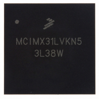
MCIMX31LVKN5 Freescale Semiconductor, MCIMX31LVKN5 Datasheet - Page 54

MCIMX31LVKN5
Manufacturer Part Number
MCIMX31LVKN5
Description
IC MPU MAP I.MX31L 457-MAPBGA
Manufacturer
Freescale Semiconductor
Series
i.MX31r
Datasheet
1.MCIMX31LITEKITC.pdf
(122 pages)
Specifications of MCIMX31LVKN5
Core Processor
ARM11
Core Size
32-Bit
Speed
532MHz
Connectivity
1-Wire, ATA, EBI/EMI, FIR, I²C, MMC/SD, PCMCIA, SIM, SPI, SSI, UART/USART, USB, USB OTG
Peripherals
DMA, LCD, POR, PWM, WDT
Program Memory Type
ROMless
Ram Size
16K x 8
Voltage - Supply (vcc/vdd)
1.22 V ~ 3.3 V
Oscillator Type
External
Operating Temperature
0°C ~ 70°C
Package / Case
457-MAPBGA
Lead Free Status / RoHS Status
Lead free / RoHS Compliant
Number Of I /o
-
Eeprom Size
-
Program Memory Size
-
Data Converters
-
Available stocks
Company
Part Number
Manufacturer
Quantity
Price
Company:
Part Number:
MCIMX31LVKN5
Manufacturer:
ADI
Quantity:
9 710
Company:
Part Number:
MCIMX31LVKN5
Manufacturer:
Freescale Semiconductor
Quantity:
10 000
Company:
Part Number:
MCIMX31LVKN5B
Manufacturer:
Freescale Semiconductor
Quantity:
10 000
Company:
Part Number:
MCIMX31LVKN5BR2
Manufacturer:
Freescale Semiconductor
Quantity:
10 000
Company:
Part Number:
MCIMX31LVKN5C
Manufacturer:
FREESCALE
Quantity:
1 831
Company:
Part Number:
MCIMX31LVKN5C
Manufacturer:
FREESCALE
Quantity:
748
Company:
Part Number:
MCIMX31LVKN5C
Manufacturer:
Freescale Semiconductor
Quantity:
10 000
Part Number:
MCIMX31LVKN5C
Manufacturer:
FREESCALE
Quantity:
20 000
Company:
Part Number:
MCIMX31LVKN5R2
Manufacturer:
IBM
Quantity:
284
Part Number:
MCIMX31LVKN5R2
Manufacturer:
FREESCALE
Quantity:
20 000
Electrical Characteristics
4.3.10
ETM is an ARM protocol. The timing specifications in this section are given as a guide for a TPA that
supports TRACECLK frequencies up to 133 MHz.
Figure 40
54
SD21 DQS – DQ Skew (defines the Data valid window in read cycles related to DQS).
SD22 DQS DQ HOLD time from DQS
SD23 DQS output access time from SDCLK posedge
ID
DQS (input)
DQ (input)
SDCLK
SDCLK
Figure 39. Mobile DDR SDRAM DQ versus DQS and SDCLK Read Cycle Timing Diagram
depicts the TRACECLK timings of ETM, and
ETM Electrical Specifications
SDRAM CLK and DQS related parameters are being measured from the
50% point—that is, high is defined as 50% of signal value and low is defined
as 50% of signal value.
The timing parameters are similar to the ones used in SDRAM data
sheets—that is,
are driven by the ESDCTL at the negative edge of SDCLK and the
parameters are measured at maximum memory frequency.
Table 39. Mobile DDR SDRAM Read Cycle Timing Parameters
SD23
Table 39
Figure 40. ETM TRACECLK Timing Diagram
MCIMX31/MCIMX31L Technical Data, Rev. 4.1
SD21
Data
Parameter
indicates SDRAM requirements. All output signals
SD22
Data
NOTE
Data
Table 40
Data
lists the timing parameters.
Data
Data
tDQSCK
Symbol
tDQSQ
tQH
Freescale Semiconductor
Data
Min Max Unit
2.3
—
—
Data
0.85
6.7
—
ns
ns
ns


