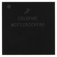
MCF5282CVF80 Freescale Semiconductor, MCF5282CVF80 Datasheet - Page 666

MCF5282CVF80
Manufacturer Part Number
MCF5282CVF80
Description
IC MPU 32BIT 66MHZ 256-MAPBGA
Manufacturer
Freescale Semiconductor
Series
MCF528xr
Datasheet
1.MCF5216CVM66J.pdf
(766 pages)
Specifications of MCF5282CVF80
Core Processor
Coldfire V2
Core Size
32-Bit
Speed
80MHz
Connectivity
CAN, EBI/EMI, Ethernet, I²C, SPI, UART/USART
Peripherals
DMA, LVD, POR, PWM, WDT
Number Of I /o
142
Program Memory Size
512KB (512K x 8)
Program Memory Type
FLASH
Ram Size
64K x 8
Voltage - Supply (vcc/vdd)
2.7 V ~ 3.6 V
Data Converters
A/D 8x10b
Oscillator Type
External
Operating Temperature
-40°C ~ 85°C
Package / Case
256-MAPBGA
Controller Family/series
ColdFire
Ram Memory Size
64KB
Embedded Interface Type
CAN, I2C, SPI, UART
No. Of Pwm Channels
8
Digital Ic Case Style
MAPBGA
Rohs Compliant
No
Package
256MA-BGA
Device Core
ColdFire
Family Name
MCF528x
Maximum Speed
80 MHz
Operating Supply Voltage
3.3 V
Data Bus Width
32 Bit
Number Of Programmable I/os
150
Interface Type
CAN/Ethernet/I2C/QSPI/UART
On-chip Adc
8-chx10-bit
Number Of Timers
12
Lead Free Status / RoHS Status
Contains lead / RoHS non-compliant
Eeprom Size
-
Available stocks
Company
Part Number
Manufacturer
Quantity
Price
Company:
Part Number:
MCF5282CVF80
Manufacturer:
FREESCALE
Quantity:
12 388
Company:
Part Number:
MCF5282CVF80
Manufacturer:
Freescale Semiconductor
Quantity:
10 000
Company:
Part Number:
MCF5282CVF80J
Manufacturer:
Freescale Semiconductor
Quantity:
10 000
- Current page: 666 of 766
- Download datasheet (9Mb)
IEEE 1149.1 Test Access Port (JTAG)
31.1
The basic features of the JTAG module are the following:
31.2
The JTAG_EN pin can select between the following modes of operation:
31.3
The JTAG module has five input and one output external signals, as described in
31.3.1
31.3.1.1 JTAG_EN — JTAG Enable
The JTAG_EN pin selects between Debug module and JTAG. If JTAG_EN is low, the Debug module is
selected; if it is high, the JTAG is selected.
upon JTAG_EN logic state.
31-2
TRST/DSCLK
TMS/BKPT
TDO/DSO
•
•
•
•
•
•
•
JTAG_EN
TDI/DSI
Name
TCLK
Performs boundary-scan operations to test circuit board electrical continuity
Bypasses instruction to reduce the shift register path to a single cell
Sets chip output pins to safety states while executing the bypass instruction
Samples the system pins during operation and transparently shift out the result
Selects between JTAG TAP controller and Background Debug Module (BDM) using a dedicated
JTAG_EN pin
JTAG mode
BDM - background debug mode (For more information, refer to
Mode
Features
Modes of Operation
External Signal Description
Detailed Signal Description
(BDM)).”
Direction
Output
Input
Input
Input
Input
Input
MCF5282 and MCF5216 ColdFire Microcontroller User’s Manual, Rev. 3
JTAG Test data output / BDM Development serial output
JTAG Test reset input / BDM Development serial clock
JTAG Test data input / BDM Development serial input
JTAG Test mode select / BDM Breakpoint
Table 31-2. Pin Function Selected
Table 31-1. Signal Properties
JTAG_EN = 0
JTAG/BDM selector input
JTAG Test clock input
Table 31-2
Function
summarizes the pin function selected depending
JTAG_EN = 1
Section 30.5, “Background Debug
Reset State
Pin Name
Hi-Z / 0
Table
—
—
—
—
—
Freescale Semiconductor
31-1.
Pull up
Active
Active
Active
Active
—
—
Related parts for MCF5282CVF80
Image
Part Number
Description
Manufacturer
Datasheet
Request
R
Part Number:
Description:
Mcf5282 And Mcf5216 Coldfire Microcontroller User�s Manual
Manufacturer:
Freescale Semiconductor, Inc
Datasheet:
Part Number:
Description:
Manufacturer:
Freescale Semiconductor, Inc
Datasheet:
Part Number:
Description:
Manufacturer:
Freescale Semiconductor, Inc
Datasheet:
Part Number:
Description:
Manufacturer:
Freescale Semiconductor, Inc
Datasheet:
Part Number:
Description:
Manufacturer:
Freescale Semiconductor, Inc
Datasheet:
Part Number:
Description:
Manufacturer:
Freescale Semiconductor, Inc
Datasheet:
Part Number:
Description:
Manufacturer:
Freescale Semiconductor, Inc
Datasheet:
Part Number:
Description:
Manufacturer:
Freescale Semiconductor, Inc
Datasheet:
Part Number:
Description:
Manufacturer:
Freescale Semiconductor, Inc
Datasheet:
Part Number:
Description:
Manufacturer:
Freescale Semiconductor, Inc
Datasheet:
Part Number:
Description:
Manufacturer:
Freescale Semiconductor, Inc
Datasheet:
Part Number:
Description:
Manufacturer:
Freescale Semiconductor, Inc
Datasheet:
Part Number:
Description:
Manufacturer:
Freescale Semiconductor, Inc
Datasheet:
Part Number:
Description:
Manufacturer:
Freescale Semiconductor, Inc
Datasheet:
Part Number:
Description:
Manufacturer:
Freescale Semiconductor, Inc
Datasheet:


