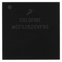
MCF5282CVF80 Freescale Semiconductor, MCF5282CVF80 Datasheet - Page 226

MCF5282CVF80
Manufacturer Part Number
MCF5282CVF80
Description
IC MPU 32BIT 66MHZ 256-MAPBGA
Manufacturer
Freescale Semiconductor
Series
MCF528xr
Datasheet
1.MCF5216CVM66J.pdf
(766 pages)
Specifications of MCF5282CVF80
Core Processor
Coldfire V2
Core Size
32-Bit
Speed
80MHz
Connectivity
CAN, EBI/EMI, Ethernet, I²C, SPI, UART/USART
Peripherals
DMA, LVD, POR, PWM, WDT
Number Of I /o
142
Program Memory Size
512KB (512K x 8)
Program Memory Type
FLASH
Ram Size
64K x 8
Voltage - Supply (vcc/vdd)
2.7 V ~ 3.6 V
Data Converters
A/D 8x10b
Oscillator Type
External
Operating Temperature
-40°C ~ 85°C
Package / Case
256-MAPBGA
Controller Family/series
ColdFire
Ram Memory Size
64KB
Embedded Interface Type
CAN, I2C, SPI, UART
No. Of Pwm Channels
8
Digital Ic Case Style
MAPBGA
Rohs Compliant
No
Package
256MA-BGA
Device Core
ColdFire
Family Name
MCF528x
Maximum Speed
80 MHz
Operating Supply Voltage
3.3 V
Data Bus Width
32 Bit
Number Of Programmable I/os
150
Interface Type
CAN/Ethernet/I2C/QSPI/UART
On-chip Adc
8-chx10-bit
Number Of Timers
12
Lead Free Status / RoHS Status
Contains lead / RoHS non-compliant
Eeprom Size
-
Available stocks
Company
Part Number
Manufacturer
Quantity
Price
Company:
Part Number:
MCF5282CVF80
Manufacturer:
FREESCALE
Quantity:
12 388
Company:
Part Number:
MCF5282CVF80
Manufacturer:
Freescale Semiconductor
Quantity:
10 000
Company:
Part Number:
MCF5282CVF80J
Manufacturer:
Freescale Semiconductor
Quantity:
10 000
- Current page: 226 of 766
- Download datasheet (9Mb)
External Interface Module (EIM)
13.3
The device uses its system clock to generate CLKOUT. Therefore, the external bus operates at the same
speed as the bus clock rate, where all bus operations are synchronous to the rising edge of CLKOUT, and
some of the bus control signals (BS, OE, and CSn,) are synchronous to the falling edge, shown in
Figure
13.4
Data transfers between the processor and other devices involve the following signals:
The address bus, write data, TS, and all attribute signals change on the rising edge of CLKOUT. Read data
is latched into the processor on the rising edge of CLKOUT.
The bus supports byte, word, and longword operand transfers and allows accesses to 8-, 16-, and 32-bit
data ports. Aspects of the transfer, such as the port size, the number of wait states for the external slave
being accessed, and whether internal transfer termination is enabled, can be programmed in the chip-select
control registers (CSCRs) and the DRAM control registers (DACRs).
Figure 13-2
if a longword is transferred for three port sizes. For example, an 8-bit memory should be connected to
D[31:24] (BS3). A longword transfer takes four transfers on D[31:24], starting with the MSB and going
to the LSB.
13-2
•
•
•
•
•
Falling-Edge
Rising-Edge
13-1. Bus characteristics may differ somewhat for interfacing with external DRAM.
Address bus (A[23:0])
Data bus (D[31:0])
Control signals (TS and TA)
CSn, OE, BS
Attribute signals (R/W, SIZ, and TIP)
CLKOUT
Bus Characteristics
Data Transfer Operation
Signals
Signals
Inputs
t
t
t
t
vo
ho
si
hi
shows the byte lanes that external memory should be connected to and the sequential transfers
= Required input setup time relative to CLKOUT edge
= Required input hold time relative to CLKOUT edge
= Propagation delay of signal relative to CLKOUT edge
= Output hold time relative to CLKOUT edge
Figure 13-1. Signal Relationship to CLKOUT for Non-DRAM Access
MCF5282 and MCF5216 ColdFire Microcontroller User’s Manual, Rev. 3
t
si
t
t
vo
hi
t
vo
t
ho
Freescale Semiconductor
t
ho
Related parts for MCF5282CVF80
Image
Part Number
Description
Manufacturer
Datasheet
Request
R
Part Number:
Description:
Mcf5282 And Mcf5216 Coldfire Microcontroller User�s Manual
Manufacturer:
Freescale Semiconductor, Inc
Datasheet:
Part Number:
Description:
Manufacturer:
Freescale Semiconductor, Inc
Datasheet:
Part Number:
Description:
Manufacturer:
Freescale Semiconductor, Inc
Datasheet:
Part Number:
Description:
Manufacturer:
Freescale Semiconductor, Inc
Datasheet:
Part Number:
Description:
Manufacturer:
Freescale Semiconductor, Inc
Datasheet:
Part Number:
Description:
Manufacturer:
Freescale Semiconductor, Inc
Datasheet:
Part Number:
Description:
Manufacturer:
Freescale Semiconductor, Inc
Datasheet:
Part Number:
Description:
Manufacturer:
Freescale Semiconductor, Inc
Datasheet:
Part Number:
Description:
Manufacturer:
Freescale Semiconductor, Inc
Datasheet:
Part Number:
Description:
Manufacturer:
Freescale Semiconductor, Inc
Datasheet:
Part Number:
Description:
Manufacturer:
Freescale Semiconductor, Inc
Datasheet:
Part Number:
Description:
Manufacturer:
Freescale Semiconductor, Inc
Datasheet:
Part Number:
Description:
Manufacturer:
Freescale Semiconductor, Inc
Datasheet:
Part Number:
Description:
Manufacturer:
Freescale Semiconductor, Inc
Datasheet:
Part Number:
Description:
Manufacturer:
Freescale Semiconductor, Inc
Datasheet:


