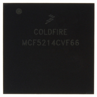
MCF5214CVF66 Freescale Semiconductor, MCF5214CVF66 Datasheet - Page 594

MCF5214CVF66
Manufacturer Part Number
MCF5214CVF66
Description
IC MPU 32BIT COLDF 256-MAPBGA
Manufacturer
Freescale Semiconductor
Series
MCF521xr
Datasheet
1.MCF5216CVM66J.pdf
(766 pages)
Specifications of MCF5214CVF66
Core Processor
Coldfire V2
Core Size
32-Bit
Speed
66MHz
Connectivity
CAN, EBI/EMI, I²C, SPI, UART/USART
Peripherals
DMA, LVD, POR, PWM, WDT
Number Of I /o
142
Program Memory Size
256KB (256K x 8)
Program Memory Type
FLASH
Ram Size
64K x 8
Voltage - Supply (vcc/vdd)
2.7 V ~ 3.6 V
Data Converters
A/D 8x12b
Oscillator Type
Internal
Operating Temperature
-40°C ~ 85°C
Package / Case
256-MAPBGA
Package
256MA-BGA
Device Core
ColdFire
Family Name
MCF521x
Maximum Speed
66 MHz
Operating Supply Voltage
3.3 V
Data Bus Width
32 Bit
Number Of Programmable I/os
142
Interface Type
QSPI/UART/I2C/CAN
On-chip Adc
8-chx10-bit
Number Of Timers
8
Lead Free Status / RoHS Status
Contains lead / RoHS non-compliant
Eeprom Size
-
Available stocks
Company
Part Number
Manufacturer
Quantity
Price
Company:
Part Number:
MCF5214CVF66
Manufacturer:
Freescale Semiconductor
Quantity:
10 000
Company:
Part Number:
MCF5214CVF66J
Manufacturer:
Freescale Semiconductor
Quantity:
10 000
- Current page: 594 of 766
- Download datasheet (9Mb)
Queued Analog-to-Digital Converter (QADC)
While there is only one result word table, the half-word (16-bit) data can be accessed in three different data
formats:
The left justified, signed format corresponds to a half-scale, offset binary, two’s complement data format.
The address used to read the result table determines the data alignment format. All write operations to the
result word table are right justified.
28.9
The QADC requires accurate, noise-free input signals for proper operation. This section discusses the
design of external circuitry to maximize QADC performance.
28.9.1
No A/D converter can be more accurate than its analog reference. Any noise in the reference can result in
at least that much error in a conversion. The reference for the QADC, supplied by signals V
should be low-pass filtered from its source to obtain a noise-free, clean signal. In many cases, simple
capacitive bypassing may suffice. In extreme cases, inductors or ferrite beads may be necessary if noise or
RF energy is present. External resistance may introduce error in this architecture under certain conditions.
Any series devices in the filter network should contain a minimum amount of DC resistance.
For accurate conversion results, the analog reference voltages must be within the limits defined by V
and V
28.9.2
The analog supply signals (V
V
28-56
RL
•
•
•
) and of the analog multiplexer inputs.
SSA
Right justified with 0s in the higher order unused bits
Left justified with the most significant bit inverted to form a sign bit, and 0s in the unused lower
order bits
Left justified with 0s in the lower order unused bits
, as explained in this subsection.
Signal Connection Considerations
Analog Reference Signals
Analog Power Signals
Although the result RAM can be written, some write operations, like bit
manipulation, may not operate as expected because the hardware cannot
access a true 16-bit value.
MCF5282 and MCF5216 ColdFire Microcontroller User’s Manual, Rev. 3
DDA
and V
SSA
Figure 28-44
) define the limits of the analog reference voltages (V
NOTE
is a diagram of the analog input circuitry.
Freescale Semiconductor
RH
and V
RH
DDA
and
RL
,
Related parts for MCF5214CVF66
Image
Part Number
Description
Manufacturer
Datasheet
Request
R
Part Number:
Description:
Manufacturer:
Freescale Semiconductor, Inc
Datasheet:
Part Number:
Description:
Manufacturer:
Freescale Semiconductor, Inc
Datasheet:
Part Number:
Description:
Manufacturer:
Freescale Semiconductor, Inc
Datasheet:
Part Number:
Description:
Manufacturer:
Freescale Semiconductor, Inc
Datasheet:
Part Number:
Description:
Manufacturer:
Freescale Semiconductor, Inc
Datasheet:
Part Number:
Description:
Manufacturer:
Freescale Semiconductor, Inc
Datasheet:
Part Number:
Description:
Manufacturer:
Freescale Semiconductor, Inc
Datasheet:
Part Number:
Description:
Manufacturer:
Freescale Semiconductor, Inc
Datasheet:
Part Number:
Description:
Manufacturer:
Freescale Semiconductor, Inc
Datasheet:
Part Number:
Description:
Manufacturer:
Freescale Semiconductor, Inc
Datasheet:
Part Number:
Description:
Manufacturer:
Freescale Semiconductor, Inc
Datasheet:
Part Number:
Description:
Manufacturer:
Freescale Semiconductor, Inc
Datasheet:
Part Number:
Description:
Manufacturer:
Freescale Semiconductor, Inc
Datasheet:
Part Number:
Description:
Manufacturer:
Freescale Semiconductor, Inc
Datasheet:
Part Number:
Description:
Manufacturer:
Freescale Semiconductor, Inc
Datasheet:


