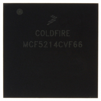
MCF5214CVF66 Freescale Semiconductor, MCF5214CVF66 Datasheet - Page 547

MCF5214CVF66
Manufacturer Part Number
MCF5214CVF66
Description
IC MPU 32BIT COLDF 256-MAPBGA
Manufacturer
Freescale Semiconductor
Series
MCF521xr
Datasheet
1.MCF5216CVM66J.pdf
(766 pages)
Specifications of MCF5214CVF66
Core Processor
Coldfire V2
Core Size
32-Bit
Speed
66MHz
Connectivity
CAN, EBI/EMI, I²C, SPI, UART/USART
Peripherals
DMA, LVD, POR, PWM, WDT
Number Of I /o
142
Program Memory Size
256KB (256K x 8)
Program Memory Type
FLASH
Ram Size
64K x 8
Voltage - Supply (vcc/vdd)
2.7 V ~ 3.6 V
Data Converters
A/D 8x12b
Oscillator Type
Internal
Operating Temperature
-40°C ~ 85°C
Package / Case
256-MAPBGA
Package
256MA-BGA
Device Core
ColdFire
Family Name
MCF521x
Maximum Speed
66 MHz
Operating Supply Voltage
3.3 V
Data Bus Width
32 Bit
Number Of Programmable I/os
142
Interface Type
QSPI/UART/I2C/CAN
On-chip Adc
8-chx10-bit
Number Of Timers
8
Lead Free Status / RoHS Status
Contains lead / RoHS non-compliant
Eeprom Size
-
Available stocks
Company
Part Number
Manufacturer
Quantity
Price
Company:
Part Number:
MCF5214CVF66
Manufacturer:
Freescale Semiconductor
Quantity:
10 000
Company:
Part Number:
MCF5214CVF66J
Manufacturer:
Freescale Semiconductor
Quantity:
10 000
- Current page: 547 of 766
- Download datasheet (9Mb)
Note: The reset value for these fields is the current signal state if DDR is an input; otherwise, they are undefined.
28.6.4
DDRQA and DDRQB are associated with port QA and QB digital I/O signals. Setting a bit in these
registers configures the corresponding signal as an output. Clearing a bit in these registers configures the
corresponding signal as an input. During QADC initialization, port QA and QB signals that will be used
as direct or multiplexed analog inputs must have their corresponding data direction register bits cleared.
When a port QA or QB signal that is programmed as an output is selected for analog conversion, the
voltage sampled is that of the output digital driver as influenced by the load.
When the MUX (externally multiplexed) bit is set in QACR0, the data direction register settings are
ignored for the bits corresponding to PQA[1:0], and the two multiplexed address (MA[1:0]) output signals.
The MA[1:0] signals are forced to be digital outputs, regardless of their data direction setting, and the
multiplexed address outputs are driven. The data returned during a port data register read is the value of
the MA[1:0] signals, regardless of their data direction setting.
Similarly, when the external trigger signals are assigned to port signals and external trigger queue
operating mode is selected, the data direction setting for the corresponding signals, PQA3 and/or PQA4,
is ignored. The port signals are forced to be digital inputs for ETRIG1 and/or ETRIG2. The data returned
during a port data register read is the value of the ETRIG[2:1] signals, regardless of their data direction
setting.
Freescale Semiconductor
Address
Address
Reset
Reset
R/W:
R/W:
Field
Field
Port QA and QB Data Direction Register (DDRQA & DDRQB)
Use caution when mixing digital and analog inputs. They should be isolated
as much as possible. Rise and fall times should be as large as possible to
minimize ac coupling effects.
7
7
Figure 28-6. QADC Port QA Data Direction Register (DDRQA)
MCF5282 and MCF5216 ColdFire Microcontroller User’s Manual, Rev. 3
Figure 28-5. QADC Port QB Data Register (PORTQB)
—
R
6
6
0000
—
R
5
5
IPSBAR + 0x19_0007
IPSBAR + 0x19_0008
DDQA4
NOTE
4
4
0000_0000
R/W
DDQA3
PQB3
(AN3)
(ANZ)
3
3
PQB2
(ANY)
(AN2)
Queued Analog-to-Digital Converter (QADC)
—
R
2
2
See Note
R/W
DDQA1
(ANX)
PQA1
(AN1)
1
1
R/W
DDQA0
(ANW)
PQA0
(AN0)
0
0
28-9
Related parts for MCF5214CVF66
Image
Part Number
Description
Manufacturer
Datasheet
Request
R
Part Number:
Description:
Manufacturer:
Freescale Semiconductor, Inc
Datasheet:
Part Number:
Description:
Manufacturer:
Freescale Semiconductor, Inc
Datasheet:
Part Number:
Description:
Manufacturer:
Freescale Semiconductor, Inc
Datasheet:
Part Number:
Description:
Manufacturer:
Freescale Semiconductor, Inc
Datasheet:
Part Number:
Description:
Manufacturer:
Freescale Semiconductor, Inc
Datasheet:
Part Number:
Description:
Manufacturer:
Freescale Semiconductor, Inc
Datasheet:
Part Number:
Description:
Manufacturer:
Freescale Semiconductor, Inc
Datasheet:
Part Number:
Description:
Manufacturer:
Freescale Semiconductor, Inc
Datasheet:
Part Number:
Description:
Manufacturer:
Freescale Semiconductor, Inc
Datasheet:
Part Number:
Description:
Manufacturer:
Freescale Semiconductor, Inc
Datasheet:
Part Number:
Description:
Manufacturer:
Freescale Semiconductor, Inc
Datasheet:
Part Number:
Description:
Manufacturer:
Freescale Semiconductor, Inc
Datasheet:
Part Number:
Description:
Manufacturer:
Freescale Semiconductor, Inc
Datasheet:
Part Number:
Description:
Manufacturer:
Freescale Semiconductor, Inc
Datasheet:
Part Number:
Description:
Manufacturer:
Freescale Semiconductor, Inc
Datasheet:


