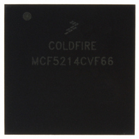
MCF5214CVF66 Freescale Semiconductor, MCF5214CVF66 Datasheet - Page 461

MCF5214CVF66
Manufacturer Part Number
MCF5214CVF66
Description
IC MPU 32BIT COLDF 256-MAPBGA
Manufacturer
Freescale Semiconductor
Series
MCF521xr
Datasheet
1.MCF5216CVM66J.pdf
(766 pages)
Specifications of MCF5214CVF66
Core Processor
Coldfire V2
Core Size
32-Bit
Speed
66MHz
Connectivity
CAN, EBI/EMI, I²C, SPI, UART/USART
Peripherals
DMA, LVD, POR, PWM, WDT
Number Of I /o
142
Program Memory Size
256KB (256K x 8)
Program Memory Type
FLASH
Ram Size
64K x 8
Voltage - Supply (vcc/vdd)
2.7 V ~ 3.6 V
Data Converters
A/D 8x12b
Oscillator Type
Internal
Operating Temperature
-40°C ~ 85°C
Package / Case
256-MAPBGA
Package
256MA-BGA
Device Core
ColdFire
Family Name
MCF521x
Maximum Speed
66 MHz
Operating Supply Voltage
3.3 V
Data Bus Width
32 Bit
Number Of Programmable I/os
142
Interface Type
QSPI/UART/I2C/CAN
On-chip Adc
8-chx10-bit
Number Of Timers
8
Lead Free Status / RoHS Status
Contains lead / RoHS non-compliant
Eeprom Size
-
Available stocks
Company
Part Number
Manufacturer
Quantity
Price
Company:
Part Number:
MCF5214CVF66
Manufacturer:
Freescale Semiconductor
Quantity:
10 000
Company:
Part Number:
MCF5214CVF66J
Manufacturer:
Freescale Semiconductor
Quantity:
10 000
- Current page: 461 of 766
- Download datasheet (9Mb)
24.3
The I
I
The logic AND function is exercised on both lines with external pull-up resistors.
Out of reset, the I
responding to a slave transmit address, the I
Section 24.4.1, “Initialization Sequence,”
Normally, a standard communication is composed of four parts: START signal, slave address transmission,
data transfer, and STOP signal. These are discussed in the following sections.
24.3.1
When no other device is bus master (I2C_SCL and I2C_SDA lines are at logic high), a device can initiate
communication by sending a START signal (see A in
high-to-low transition of I2C_SDA while I2C_SCL is high. This signal denotes the beginning of a data
transfer (each data transfer can be several bytes long) and awakens all slaves.
Freescale Semiconductor
2
C compliance, all devices connected to these two signals must have open drain or open collector outputs.
Field
DATA
7–0
IPSBAR
2
C module uses a serial data line (I2C_SDA) and a serial clock line (I2C_SCL) for data transfer. For
Offset:
Reset:
I
bit is sent first. In master receive mode, reading this register initiates the reception of the next byte of data. In slave
mode, the same functions are available after an address match has occurred.
Note: In master transmit mode, the first byte of data written to I2DR following assertion of I2CR[MSTA] is used for
Note: I2CR[MSTA] generates a start when a master does not already own the bus. I2CR[RSTA] generates a start
Functional Description
W
2
R
C data. When data is written to this register in master transmit mode, a data transfer is initiated. The most significant
START Signal
0x00_0310 (I2DR)
the address transfer and should comprise the calling address (in position D7–D1) concatenated with the
required R/W bit (in position D0). This bit (D0) is not automatically appended by the hardware, software must
provide the appropriate R/W bit.
(restart) without the master first issuing a stop (i.e., the master already owns the bus). To start the read of data,
a dummy read to this register starts the read process from the slave. The next read of the I2DR register
contains the actual data.
2
0
7
C default state is as a slave receiver. Therefore, when not programmed to be a master or
MCF5282 and MCF5216 ColdFire Microcontroller User’s Manual, Rev. 3
6
0
Figure 24-6. I
Table 24-6. I2DR Field Description
0
5
for exceptions.
2
C module should return to the default slave receiver state. See
2
C Data I/O Register (I2DR)
0
4
Description
Figure
DATA
24-7). A START signal is defined as a
0
3
0
2
Access: User read/write
0
1
I
2
0
0
C Interface
24-7
Related parts for MCF5214CVF66
Image
Part Number
Description
Manufacturer
Datasheet
Request
R
Part Number:
Description:
Manufacturer:
Freescale Semiconductor, Inc
Datasheet:
Part Number:
Description:
Manufacturer:
Freescale Semiconductor, Inc
Datasheet:
Part Number:
Description:
Manufacturer:
Freescale Semiconductor, Inc
Datasheet:
Part Number:
Description:
Manufacturer:
Freescale Semiconductor, Inc
Datasheet:
Part Number:
Description:
Manufacturer:
Freescale Semiconductor, Inc
Datasheet:
Part Number:
Description:
Manufacturer:
Freescale Semiconductor, Inc
Datasheet:
Part Number:
Description:
Manufacturer:
Freescale Semiconductor, Inc
Datasheet:
Part Number:
Description:
Manufacturer:
Freescale Semiconductor, Inc
Datasheet:
Part Number:
Description:
Manufacturer:
Freescale Semiconductor, Inc
Datasheet:
Part Number:
Description:
Manufacturer:
Freescale Semiconductor, Inc
Datasheet:
Part Number:
Description:
Manufacturer:
Freescale Semiconductor, Inc
Datasheet:
Part Number:
Description:
Manufacturer:
Freescale Semiconductor, Inc
Datasheet:
Part Number:
Description:
Manufacturer:
Freescale Semiconductor, Inc
Datasheet:
Part Number:
Description:
Manufacturer:
Freescale Semiconductor, Inc
Datasheet:
Part Number:
Description:
Manufacturer:
Freescale Semiconductor, Inc
Datasheet:


