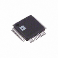
ADUC7032BSTZ-8V-RL Analog Devices Inc, ADUC7032BSTZ-8V-RL Datasheet - Page 75

ADUC7032BSTZ-8V-RL
Manufacturer Part Number
ADUC7032BSTZ-8V-RL
Description
IC BATTERY SENSOR PREC 48-LQFP
Manufacturer
Analog Devices Inc
Series
MicroConverter® ADuC7xxxr
Datasheet
1.ADUC7032BSTZ-8V-RL.pdf
(128 pages)
Specifications of ADUC7032BSTZ-8V-RL
Core Processor
ARM7
Core Size
16/32-Bit
Speed
20.48MHz
Connectivity
LIN, SPI, UART/USART
Peripherals
POR, PSM, Temp Sensor, WDT
Number Of I /o
9
Program Memory Size
96KB (96K x 8)
Program Memory Type
FLASH
Ram Size
6K x 8
Voltage - Supply (vcc/vdd)
3.5 V ~ 18 V
Data Converters
A/D 2x16b
Oscillator Type
Internal
Operating Temperature
-40°C ~ 105°C
Package / Case
48-LQFP
Lead Free Status / RoHS Status
Lead free / RoHS Compliant
Eeprom Size
-
Other names
ADUC7032BSTZ-8V-RLCT
Available stocks
Company
Part Number
Manufacturer
Quantity
Price
Company:
Part Number:
ADUC7032BSTZ-8V-RL
Manufacturer:
Analog Devices Inc
Quantity:
10 000
Preliminary Technical Data
PROCESSOR REFERENCE PERIPHERALS
INTERRUPT SYSTEM
There are 15 interrupt sources on the ADuC7032 which are
controlled by the Interrupt Controller. Most interrupts are
generated from the on-chip peripherals such as the ADC,
UART, etc.. The ARM7TDMI CPU core will only recognize
interrupts as one of two types, a normal interrupt request IRQ
and a fast interrupt request FIQ. All the interrupts can be
masked separately.
The control and configuration of the interrupt system is
managed through nine interrupt-related registers, four
dedicated to IRQ, four dedicated to FIQ. An additional MMR is
used to select the programmed interrupt source. The bits in
each IRQ and FIQ registers represent the same interrupt source
as described in Table 41.
IRQSTA/FIQSTA should be saved immediately upon entering
the ISR ( Interrupt Service Routine ) to ensure that all valid
interrupt sources are serviced.
The interrupt generation route through the ARM7TDMI core
is shown in Figure 29.
Bit
10
11
12
13
14
15
16
17
18
0
1
2
3
4
5
6
7
8
9
Description
All interrupts OR’ e d
SWI:
not used in IRQEN/CLR and FIQEN/CLR
Timer 0
Timer 1
Timer 2 - Wake Up timer
Timer 3 - Watchdog Timer
Reserved and should be written as zero
LIN Hardware
Flash/EE Interrupt
PLL Lock
ADC
UART
SPI
XIRQ0
XIRQ1
Reserved and should be written as zero
IRQ3 High Voltage IRQ
XIRQ4
XIRQ5
( GPIO IRQ 0 )
( GPIO IRQ 1 )
( GPIO IRQ 4 )
( GPIO IRQ 5 )
Table 41 : IRQ/FIQ MMRs bit description
Rev. PrD | Page 75 of 128
For more information please refer to:
Timer0 – Life-Time timer Page 78
Timer1 Page 79
Timer2 - Wake-Up Timer Page 82
Timer3 - Watchdog Timer Page 83
LIN (Local Interconnect Network ) INTERFACE Page 115
Flash/EE memory Control Interface Page 31
ADuC7032 System Clocks Page 68
16-Bit Σ−∆ Analog to Digital Converters Page 44
UART SERIAL INTERFACE Page 105
SERIAL PERIPHERAL INTERFACE Page 112
General Purpose I/O Page 84
General Purpose I/O Page 84
High Voltage Interrupt
General Purpose I/O Page 84
General Purpose I/O Page 84
Consider the example of Timer0 which is configured to
generate a timeout every 1ms.
After the first 1ms timeout, FIQSIG/IRQSIG[2] will be set and
will only be cleared by writing to T0CLRI.
If Timer0 is not enabled in either IRQEN or FIQEN, then
FIQSTA/IRQSTA[2] will not be set and an interrupt will not
occur.
If Timer0 is enabled in either IRQEN or FIQEN, then either
FIQSTA/IRQSTA[2] will be set and either an FIQ or an IRQ
interrupt will occur.
Please note that the IRQ and FIQ interrupt bit definitions in the
CPSR only control interrupt recognition by the ARM Core, not
by the peripherals.
For example, if Timer2 is confirgured to generate an IRQ via
IRQEN, the IRQ interrupt bit is set ( Disabled ) in the CPSR
and the ADuC7032 is powered down. When an interrupt
occurs, the peripherals will be woken, but the ARM core will
remain powered down. This is equivalent to POWCON = 0x71.
The ARM Core can only be powered up by a reset event if this
occurs.
ADuC7032


