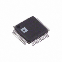
ADUC7032BSTZ-8V-RL Analog Devices Inc, ADUC7032BSTZ-8V-RL Datasheet - Page 115

ADUC7032BSTZ-8V-RL
Manufacturer Part Number
ADUC7032BSTZ-8V-RL
Description
IC BATTERY SENSOR PREC 48-LQFP
Manufacturer
Analog Devices Inc
Series
MicroConverter® ADuC7xxxr
Datasheet
1.ADUC7032BSTZ-8V-RL.pdf
(128 pages)
Specifications of ADUC7032BSTZ-8V-RL
Core Processor
ARM7
Core Size
16/32-Bit
Speed
20.48MHz
Connectivity
LIN, SPI, UART/USART
Peripherals
POR, PSM, Temp Sensor, WDT
Number Of I /o
9
Program Memory Size
96KB (96K x 8)
Program Memory Type
FLASH
Ram Size
6K x 8
Voltage - Supply (vcc/vdd)
3.5 V ~ 18 V
Data Converters
A/D 2x16b
Oscillator Type
Internal
Operating Temperature
-40°C ~ 105°C
Package / Case
48-LQFP
Lead Free Status / RoHS Status
Lead free / RoHS Compliant
Eeprom Size
-
Other names
ADUC7032BSTZ-8V-RLCT
Available stocks
Company
Part Number
Manufacturer
Quantity
Price
Company:
Part Number:
ADUC7032BSTZ-8V-RL
Manufacturer:
Analog Devices Inc
Quantity:
10 000
Preliminary Technical Data
LIN (LOCAL INTERCONNECT NETWORK ) INTERFACE
The ADuC7032 features a high voltage physical interface
between the ARM7 MCU core and an external LIN bus. The
LIN interface operates as a slave only interface, operating from
1-20KBaud, and is compatible with the LIN2.0 standard. The
pull-up resistor required for a slave node is on-chip, reducing
the need for external circuitry. The LIN protocol is emulated
using the on-chip UART, an IRQ, a dedicated LIN Timer and
the high voltage transceiver which is also incorporated on-chip.
This is shown in Figure 38. The LIN is clocked from the Low
Power Oscillator, for the Break Timer, and a 5MHz output from
the PLL which is used for the synch byte timing.
LHS INTERRUPT
IRQEN[7]
GP2DAT[29
GP2DAT21
GPIO12
131KHz
&
5MHz
HARDWARE
ADuC7032
ADuC7032
LHSVAL0
LHSVAL1
UART
LHS
RxD ENABLE
RxD
LHSCON0[8]
TxD
GP2CON[20]
FUNCTION
SELECT
GPIO12
INTERRUPT
LOGIC
LHS
BREAK LHSSTA[0]
START LHSSTA[1]
STOP LHSSTA[2]
BREAK
ERROR LHSSTA[4]
DISABLE
OUTPUT
SHORT-CIRCUIT
INTERRUPT
SOURCES
FOUR LIN
HVCFG1[2]
CONTROL
Figure 38 : LIN I/O, Block Diagram
HVCFG0[1:0]
LIN MODE
Rev. PrD | Page 115 of 128
LIN ENABLE
(INTERNAL
HVCFG0[5]
TRIP REFERENCE
PULL-UP)
SHORT-CIRCUIT
THRESHOLD
REFERENCE
INTERNAL
VOLTAGE
INPUT
LIN MMR DESCRIPTION
The LIN Hardware Synchronization (LHS) functionality is
controlled via five MMRs. The function of each MMR is
described below:.
LHSSTA:
LHSCON0:
LHSCON1:
LHSVAL0:
LHSVAL1:
VDD
X
RESISTOR
INTERNAL
CIRCUIT
SHORT
SENSE
LHS Status Register. This MMR contains
information flags which describe the current
status on the interface.
LHS Control Register 0. This MMR controls the
configuration of the LHS Timer.
LHS Start and Stop Edge Control Register
Dictates which edge of the LIN Synchronization
byte the LHS starts/stops counting.
LHS Synchronization 16Bit Timer, which is
controlled by LHSCON0.
LHS Break Timer Register
SCR
IO_VSS
PROTECTION
VOLATGE
OVER
EXTERNAL
LIN PIN
ADuC7032
VDD
MASTER ECU
PROTECTION
MASTER ECU
C LOAD
PULL-UP
DIODE


