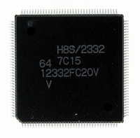
D12332VFC20V Renesas Electronics America, D12332VFC20V Datasheet - Page 943

D12332VFC20V
Manufacturer Part Number
D12332VFC20V
Description
IC H8S/2332 MCU ROMLESS 144QFP
Manufacturer
Renesas Electronics America
Series
H8® H8S/2300r
Specifications of D12332VFC20V
Core Processor
H8S/2000
Core Size
16-Bit
Speed
20MHz
Connectivity
SCI, SmartCard
Peripherals
DMA, POR, PWM, WDT
Number Of I /o
106
Program Memory Type
ROMless
Ram Size
8K x 8
Voltage - Supply (vcc/vdd)
2.7 V ~ 3.6 V
Data Converters
A/D 12x10b; D/A 4x8b
Oscillator Type
Internal
Operating Temperature
-20°C ~ 75°C
Package / Case
144-QFP
For Use With
EDK2329 - DEV EVALUATION KIT H8S/2329
Lead Free Status / RoHS Status
Lead free / RoHS Compliant
Eeprom Size
-
Program Memory Size
-
Available stocks
Company
Part Number
Manufacturer
Quantity
Price
Company:
Part Number:
D12332VFC20V
Manufacturer:
Renesas Electronics America
Quantity:
10 000
- Current page: 943 of 1246
- Download datasheet (7Mb)
Notes: 1. Follow the program/erase algorithms when making the time settings.
22.3
Although both the F-ZTAT and mask ROM versions fully meet the electrical specifications listed
in this manual, there may be differences in the actual values of the electrical characteristics,
operating margins, noise margins, and so forth, due to differences in the fabrication process, the
on-chip ROM, and the layout patterns.
If the F-ZTAT version is used to carry out system evaluation and testing, therefore, when
switching to the mask ROM version the same evaluation and testing procedures should also be
conducted on this version.
2. Programming time per 128 bytes. (Indicates the total time during which the P bit is set
3. Time to erase one block. (Indicates the time during which the E bit is set in FLMCR1.
4. Maximum programming time
5. The maximum number of writes (N) should be set as shown below according to the
6. For the maximum erase time (t
7. Minimum number of times for which all characteristics are guaranteed after rewriting
8. Reference value for 25°C (as a guideline, rewriting should normally function up to this
9. Data retention characteristic when rewriting is performed within the specification range,
Usage Note
The wait time after P bit setting (z) should be changed as follows according to the
Number of writes (n)
in flash memory control register 1 (FLMCR1). Does not include the program-verify
time.)
Does not include the erase-verify time.)
actual set value of z so as not to exceed the maximum programming time (t
number of writes (n).
wait time after E bit setting (z) and the maximum number of erases (N):
(Guarantee range is 1 to minimum value).
value).
including the minimum value.
t
1 ≤ n ≤ 6
7 ≤ n ≤ 1000
1 ≤ n ≤ 6
t
P
E
(max) =
(max) = Wait time after E bit setting (z) × maximum number of erases (N)
i=1
Σ
N
wait time after P bit setting (z)
z = 30 µs
z = 200 µs
z = 10 µs: For additional writing
E
(max)), the following relationship applies between the
Rev.4.00 Sep. 07, 2007 Page 911 of 1210
REJ09B0245-0400
P
(max)).
Related parts for D12332VFC20V
Image
Part Number
Description
Manufacturer
Datasheet
Request
R

Part Number:
Description:
KIT STARTER FOR M16C/29
Manufacturer:
Renesas Electronics America
Datasheet:

Part Number:
Description:
KIT STARTER FOR R8C/2D
Manufacturer:
Renesas Electronics America
Datasheet:

Part Number:
Description:
R0K33062P STARTER KIT
Manufacturer:
Renesas Electronics America
Datasheet:

Part Number:
Description:
KIT STARTER FOR R8C/23 E8A
Manufacturer:
Renesas Electronics America
Datasheet:

Part Number:
Description:
KIT STARTER FOR R8C/25
Manufacturer:
Renesas Electronics America
Datasheet:

Part Number:
Description:
KIT STARTER H8S2456 SHARPE DSPLY
Manufacturer:
Renesas Electronics America
Datasheet:

Part Number:
Description:
KIT STARTER FOR R8C38C
Manufacturer:
Renesas Electronics America
Datasheet:

Part Number:
Description:
KIT STARTER FOR R8C35C
Manufacturer:
Renesas Electronics America
Datasheet:

Part Number:
Description:
KIT STARTER FOR R8CL3AC+LCD APPS
Manufacturer:
Renesas Electronics America
Datasheet:

Part Number:
Description:
KIT STARTER FOR RX610
Manufacturer:
Renesas Electronics America
Datasheet:

Part Number:
Description:
KIT STARTER FOR R32C/118
Manufacturer:
Renesas Electronics America
Datasheet:

Part Number:
Description:
KIT DEV RSK-R8C/26-29
Manufacturer:
Renesas Electronics America
Datasheet:

Part Number:
Description:
KIT STARTER FOR SH7124
Manufacturer:
Renesas Electronics America
Datasheet:

Part Number:
Description:
KIT STARTER FOR H8SX/1622
Manufacturer:
Renesas Electronics America
Datasheet:

Part Number:
Description:
KIT DEV FOR SH7203
Manufacturer:
Renesas Electronics America
Datasheet:


