D12332VFC20V Renesas Electronics America, D12332VFC20V Datasheet - Page 311
D12332VFC20V
Manufacturer Part Number
D12332VFC20V
Description
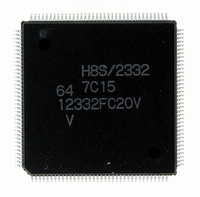
IC H8S/2332 MCU ROMLESS 144QFP
Manufacturer
Renesas Electronics America
Series
H8® H8S/2300r
Specifications of D12332VFC20V
Core Processor
H8S/2000
Core Size
16-Bit
Speed
20MHz
Connectivity
SCI, SmartCard
Peripherals
DMA, POR, PWM, WDT
Number Of I /o
106
Program Memory Type
ROMless
Ram Size
8K x 8
Voltage - Supply (vcc/vdd)
2.7 V ~ 3.6 V
Data Converters
A/D 12x10b; D/A 4x8b
Oscillator Type
Internal
Operating Temperature
-20°C ~ 75°C
Package / Case
144-QFP
For Use With
EDK2329 - DEV EVALUATION KIT H8S/2329
Lead Free Status / RoHS Status
Lead free / RoHS Compliant
Eeprom Size
-
Program Memory Size
-
Available stocks
Company
Part Number
Manufacturer
Quantity
Price
Company:

Part Number:
D12332VFC20V
Manufacturer:
Renesas Electronics America
Quantity:
10 000


DREQ Pin Falling Edge Activation Timing: Set the DTA bit for the channel for which the
DREQ pin is selected to 1.
Figure 7.31 shows an example of DREQ pin falling edge activated single address mode transfer.
DREQ pin sampling is performed every cycle, with the rising edge of the next φ cycle after the
end of the DMABCR write cycle for setting the transfer enabled state as the starting point.
When the DREQ pin low level is sampled while acceptance by means of the DREQ pin is
possible, the request is held in the DMAC. Then, when activation is initiated in the DMAC, the
request is cleared, and DREQ pin high level sampling for edge detection is started. If DREQ pin
high level sampling has been completed by the time the DMA single cycle ends, acceptance
Figure 7.31 Example of DREQ Pin Falling Edge Activated Single Address Mode Transfer
Address bus
[1]
[2] [5] The request is cleared at the next bus break, and activation is started in the DMAC.
[3] [6] Start of DMA cycle; DREQ pin high level sampling on the rising edge of φ starts.
[4] [7] When the DREQ pin high level has been sampled, acceptance is resumed after the single
Note: In write data buffer mode, bus breaks from [2] to [7] may be hidden, and not visible.
DMA control
Channel
DREQ
DACK
Acceptance after transfer enabling; the DREQ pin low level is sampled on the rising edge of φ,
and the request is held.
cycle is completed. (As in [1], the DREQ pin low level is sampled on the rising edge of φ, and
the request is held.)
φ
Idle
[1]
Request
Bus release
Minimum of
2 cycles
[2]
[3]
Single
Request clear
Transfer source/
DMA single
period
destination
Acceptance resumes
Idle
[4]
Request
Bus release
Rev.4.00 Sep. 07, 2007 Page 279 of 1210
Minimum of
2 cycles
[5]
[6]
Single
DMA single
Request clear
Transfer source/
destination
period
Acceptance resumes
Idle
[7]
REJ09B0245-0400
Bus release
Related parts for D12332VFC20V
Image
Part Number
Description
Manufacturer
Datasheet
Request
R

Part Number:
Description:
KIT STARTER FOR M16C/29
Manufacturer:
Renesas Electronics America
Datasheet:

Part Number:
Description:
KIT STARTER FOR R8C/2D
Manufacturer:
Renesas Electronics America
Datasheet:

Part Number:
Description:
R0K33062P STARTER KIT
Manufacturer:
Renesas Electronics America
Datasheet:

Part Number:
Description:
KIT STARTER FOR R8C/23 E8A
Manufacturer:
Renesas Electronics America
Datasheet:

Part Number:
Description:
KIT STARTER FOR R8C/25
Manufacturer:
Renesas Electronics America
Datasheet:

Part Number:
Description:
KIT STARTER H8S2456 SHARPE DSPLY
Manufacturer:
Renesas Electronics America
Datasheet:

Part Number:
Description:
KIT STARTER FOR R8C38C
Manufacturer:
Renesas Electronics America
Datasheet:

Part Number:
Description:
KIT STARTER FOR R8C35C
Manufacturer:
Renesas Electronics America
Datasheet:

Part Number:
Description:
KIT STARTER FOR R8CL3AC+LCD APPS
Manufacturer:
Renesas Electronics America
Datasheet:
Part Number:
Description:
KIT STARTER FOR RX610
Manufacturer:
Renesas Electronics America
Datasheet:

Part Number:
Description:
KIT STARTER FOR R32C/118
Manufacturer:
Renesas Electronics America
Datasheet:

Part Number:
Description:
KIT DEV RSK-R8C/26-29
Manufacturer:
Renesas Electronics America
Datasheet:

Part Number:
Description:
KIT STARTER FOR SH7124
Manufacturer:
Renesas Electronics America
Datasheet:

Part Number:
Description:
KIT STARTER FOR H8SX/1622
Manufacturer:
Renesas Electronics America
Datasheet:

Part Number:
Description:
KIT DEV FOR SH7203
Manufacturer:
Renesas Electronics America
Datasheet: