MC908GT16CBE Freescale Semiconductor, MC908GT16CBE Datasheet - Page 228
MC908GT16CBE
Manufacturer Part Number
MC908GT16CBE
Description
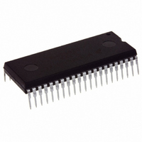
IC MCU 16K FLASH 8MHZ SPI 42SDIP
Manufacturer
Freescale Semiconductor
Series
HC08r
Datasheet
1.MC908GT8CFBE.pdf
(292 pages)
Specifications of MC908GT16CBE
Core Processor
HC08
Core Size
8-Bit
Speed
8MHz
Connectivity
SCI, SPI
Peripherals
LVD, POR, PWM
Number Of I /o
36
Program Memory Size
16KB (16K x 8)
Program Memory Type
FLASH
Ram Size
512 x 8
Voltage - Supply (vcc/vdd)
2.7 V ~ 5.5 V
Data Converters
A/D 8x8b
Oscillator Type
Internal
Operating Temperature
-40°C ~ 85°C
Package / Case
42-DIP (0.600", 15.24mm)
Controller Family/series
HC08
No. Of I/o's
34
Ram Memory Size
512Byte
Cpu Speed
8MHz
No. Of Timers
2
Embedded Interface Type
I2C, SCI, SPI
Rohs Compliant
Yes
Processor Series
HC08GT
Core
HC08
Data Bus Width
8 bit
Data Ram Size
512 B
Interface Type
SCI, SPI
Maximum Clock Frequency
8 MHz
Number Of Programmable I/os
30
Number Of Timers
4
Operating Supply Voltage
0 V to 5 V
Maximum Operating Temperature
+ 85 C
Mounting Style
Through Hole
Development Tools By Supplier
FSICEBASE, DEMO908GZ60E, M68CBL05CE, M68EML08GPGTE
Minimum Operating Temperature
- 40 C
On-chip Adc
8 bit, 8 Channel
Package
42SPDIP
Family Name
HC08
Maximum Speed
8 MHz
Lead Free Status / RoHS Status
Lead free / RoHS Compliant
Eeprom Size
-
Lead Free Status / Rohs Status
Details


Timer Interface Module (TIM)
18.4.4.2 Buffered PWM Signal Generation
Channels 0 and 1 can be linked to form a buffered PWM channel whose output appears on the TCH0 pin.
The TIM channel registers of the linked pair alternately control the pulse width of the output.
Setting the MS0B bit in TIM channel 0 status and control register (TSC0) links channel 0 and channel 1.
The TIM channel 0 registers initially control the pulse width on the TCH0 pin. Writing to the TIM channel 1
registers enables the TIM channel 1 registers to synchronously control the pulse width at the beginning
of the next PWM period. At each subsequent overflow, the TIM channel registers (0 or 1) that control the
pulse width are the ones written to last. TSC0 controls and monitors the buffered PWM function, and TIM
channel 1 status and control register (TSC1) is unused. While the MS0B bit is set, the channel 1 pin,
TCH1, is available as a general-purpose I/O pin.
18.4.4.3 PWM Initialization
To ensure correct operation when generating unbuffered or buffered PWM signals, use the following
initialization procedure:
228
1. In the TIM status and control register (TSC):
2. In the TIM counter modulo registers (TMODH:TMODL), write the value for the required PWM
3. In the TIM channel x registers (TCHxH:TCHxL), write the value for the required pulse width.
4. In TIM channel x status and control register (TSCx):
•
When changing to a longer pulse width, enable TIM overflow interrupts and write the new value in
the TIM overflow interrupt routine. The TIM overflow interrupt occurs at the end of the current PWM
period. Writing a larger value in an output compare interrupt routine (at the end of the current pulse)
could cause two output compares to occur in the same PWM period.
period.
a. Stop the TIM counter by setting the TIM stop bit, TSTOP.
b. Reset the TIM counter and prescaler by setting the TIM reset bit, TRST.
a. Write 0:1 (for unbuffered output compare or PWM signals) or 1:0 (for buffered output compare
b. Write 1 to the toggle-on-overflow bit, TOVx.
or PWM signals) to the mode select bits, MSxB:MSxA. (See
In PWM signal generation, do not program the PWM channel to toggle on
output compare. Toggling on output compare prevents reliable 0% duty
cycle generation and removes the ability of the channel to self-correct in the
event of software error or noise. Toggling on output compare also can
cause incorrect PWM signal generation when changing the PWM pulse
width to a new, much larger value.
In buffered PWM signal generation, do not write new pulse width values to
the currently active channel registers. User software should track the
currently active channel to prevent writing a new value to the active
channel. Writing to the active channel registers is the same as generating
unbuffered PWM signals.
MC68HC908GT16 • MC68HC908GT8 • MC68HC08GT16 Data Sheet, Rev. 5.0
NOTE
NOTE
Table
18-2.)
Freescale Semiconductor
Related parts for MC908GT16CBE
Image
Part Number
Description
Manufacturer
Datasheet
Request
R

Part Number:
Description:
Manufacturer:
Freescale Semiconductor, Inc
Datasheet:
Part Number:
Description:
Manufacturer:
Freescale Semiconductor, Inc
Datasheet:
Part Number:
Description:
Manufacturer:
Freescale Semiconductor, Inc
Datasheet:
Part Number:
Description:
Manufacturer:
Freescale Semiconductor, Inc
Datasheet:
Part Number:
Description:
Manufacturer:
Freescale Semiconductor, Inc
Datasheet:
Part Number:
Description:
Manufacturer:
Freescale Semiconductor, Inc
Datasheet:
Part Number:
Description:
Manufacturer:
Freescale Semiconductor, Inc
Datasheet:
Part Number:
Description:
Manufacturer:
Freescale Semiconductor, Inc
Datasheet:
Part Number:
Description:
Manufacturer:
Freescale Semiconductor, Inc
Datasheet:
Part Number:
Description:
Manufacturer:
Freescale Semiconductor, Inc
Datasheet:
Part Number:
Description:
Manufacturer:
Freescale Semiconductor, Inc
Datasheet:
Part Number:
Description:
Manufacturer:
Freescale Semiconductor, Inc
Datasheet:
Part Number:
Description:
Manufacturer:
Freescale Semiconductor, Inc
Datasheet:
Part Number:
Description:
Manufacturer:
Freescale Semiconductor, Inc
Datasheet:
Part Number:
Description:
Manufacturer:
Freescale Semiconductor, Inc
Datasheet: