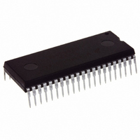
MC908GT16CBE Freescale Semiconductor, MC908GT16CBE Datasheet - Page 132

MC908GT16CBE
Manufacturer Part Number
MC908GT16CBE
Description
IC MCU 16K FLASH 8MHZ SPI 42SDIP
Manufacturer
Freescale Semiconductor
Series
HC08r
Datasheet
1.MC908GT8CFBE.pdf
(292 pages)
Specifications of MC908GT16CBE
Core Processor
HC08
Core Size
8-Bit
Speed
8MHz
Connectivity
SCI, SPI
Peripherals
LVD, POR, PWM
Number Of I /o
36
Program Memory Size
16KB (16K x 8)
Program Memory Type
FLASH
Ram Size
512 x 8
Voltage - Supply (vcc/vdd)
2.7 V ~ 5.5 V
Data Converters
A/D 8x8b
Oscillator Type
Internal
Operating Temperature
-40°C ~ 85°C
Package / Case
42-DIP (0.600", 15.24mm)
Controller Family/series
HC08
No. Of I/o's
34
Ram Memory Size
512Byte
Cpu Speed
8MHz
No. Of Timers
2
Embedded Interface Type
I2C, SCI, SPI
Rohs Compliant
Yes
Processor Series
HC08GT
Core
HC08
Data Bus Width
8 bit
Data Ram Size
512 B
Interface Type
SCI, SPI
Maximum Clock Frequency
8 MHz
Number Of Programmable I/os
30
Number Of Timers
4
Operating Supply Voltage
0 V to 5 V
Maximum Operating Temperature
+ 85 C
Mounting Style
Through Hole
Development Tools By Supplier
FSICEBASE, DEMO908GZ60E, M68CBL05CE, M68EML08GPGTE
Minimum Operating Temperature
- 40 C
On-chip Adc
8 bit, 8 Channel
Package
42SPDIP
Family Name
HC08
Maximum Speed
8 MHz
Lead Free Status / RoHS Status
Lead free / RoHS Compliant
Eeprom Size
-
Lead Free Status / Rohs Status
Details
- Current page: 132 of 292
- Download datasheet (4Mb)
Input/Output (I/O) Ports (PORTS)
PTCPUE6–PTCPUE0 — Port C Input Pullup Enable Bits
12.5 Port D
Port D is an 8-bit special-function port that shares four of its pins with the serial peripheral interface (SPI)
module and four of its pins with two timer interface (TIM1 and TIM2) modules. Port D also has software
configurable pullup devices if configured as an input port.
12.5.1 Port D Data Register
The port D data register (PTD) contains a data latch for each of the eight port D pins.
PTD7–PTD0 — Port D Data Bits
T2CH1 and T2CH0 — Timer 2 Channel I/O Bits
T1CH1 and T1CH0 — Timer 1 Channel I/O Bits
SPSCK — SPI Serial Clock
MOSI — Master Out/Slave In
MISO — Master In/Slave Out
132
These writable bits are software programmable to enable pullup devices on an input port bit.
These read/write bits are software-programmable. Data direction of each port D pin is under the control
of the corresponding bit in data direction register D. Reset has no effect on port D data.
The PTD7/T2CH1–PTD6/T2CH0 pins are the TIM2 input capture/output compare pins. The edge/level
select bits, ELSxB:ELSxA, determine whether the PTD7/T2CH1–PTD6/T2CH0 pins are timer channel
I/O pins or general-purpose I/O pins. See
The PTD7/T1CH1–PTD6/T1CH0 pins are the TIM1 input capture/output compare pins. The edge/level
select bits, ELSxB and ELSxA, determine whether the PTD7/T1CH1–PTD6/T1CH0 pins are timer
channel I/O pins or general-purpose I/O pins. See
The PTD3/SPSCK pin is the serial clock input of the SPI module. When the SPE bit is clear, the
PTD3/SPSCK pin is available for general-purpose I/O.
The PTD2/MOSI pin is the master out/slave in terminal of the SPI module. When the SPE bit is clear,
the PTD2/MOSI pin is available for general-purpose I/O.
The PTD1/MISO pin is the master in/slave out terminal of the SPI module. When the SPI enable bit,
SPE, is clear, the SPI module is disabled, and the PTD0/SS pin is available for general-purpose I/O.
1 = Corresponding port C pin configured to have internal pullup
0 = Corresponding port C pin internal pullup disconnected
Alternative Function:
Address:
Reset:
Read:
Write:
MC68HC908GT16 • MC68HC908GT8 • MC68HC08GT16 Data Sheet, Rev. 5.0
T2CH1
$0003
PTD7
Bit 7
Figure 12-13. Port D Data Register (PTD)
T2CH0
PTD6
6
T1CH1
PTD5
Chapter 18 Timer Interface Module
5
T1CH0
Unaffected by reset
PTD4
Chapter 18 Timer Interface Module
4
SPSCK
PTD3
3
PTD2
MOSI
2
PTD1
MISO
(TIM).
1
Freescale Semiconductor
PTD0
Bit 0
(TIM).
SS
Related parts for MC908GT16CBE
Image
Part Number
Description
Manufacturer
Datasheet
Request
R
Part Number:
Description:
Manufacturer:
Freescale Semiconductor, Inc
Datasheet:
Part Number:
Description:
Manufacturer:
Freescale Semiconductor, Inc
Datasheet:
Part Number:
Description:
Manufacturer:
Freescale Semiconductor, Inc
Datasheet:
Part Number:
Description:
Manufacturer:
Freescale Semiconductor, Inc
Datasheet:
Part Number:
Description:
Manufacturer:
Freescale Semiconductor, Inc
Datasheet:
Part Number:
Description:
Manufacturer:
Freescale Semiconductor, Inc
Datasheet:
Part Number:
Description:
Manufacturer:
Freescale Semiconductor, Inc
Datasheet:
Part Number:
Description:
Manufacturer:
Freescale Semiconductor, Inc
Datasheet:
Part Number:
Description:
Manufacturer:
Freescale Semiconductor, Inc
Datasheet:
Part Number:
Description:
Manufacturer:
Freescale Semiconductor, Inc
Datasheet:
Part Number:
Description:
Manufacturer:
Freescale Semiconductor, Inc
Datasheet:
Part Number:
Description:
Manufacturer:
Freescale Semiconductor, Inc
Datasheet:
Part Number:
Description:
Manufacturer:
Freescale Semiconductor, Inc
Datasheet:
Part Number:
Description:
Manufacturer:
Freescale Semiconductor, Inc
Datasheet:
Part Number:
Description:
Manufacturer:
Freescale Semiconductor, Inc
Datasheet:


