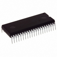
MC908GT16CBE Freescale Semiconductor, MC908GT16CBE Datasheet - Page 127

MC908GT16CBE
Manufacturer Part Number
MC908GT16CBE
Description
IC MCU 16K FLASH 8MHZ SPI 42SDIP
Manufacturer
Freescale Semiconductor
Series
HC08r
Datasheet
1.MC908GT8CFBE.pdf
(292 pages)
Specifications of MC908GT16CBE
Core Processor
HC08
Core Size
8-Bit
Speed
8MHz
Connectivity
SCI, SPI
Peripherals
LVD, POR, PWM
Number Of I /o
36
Program Memory Size
16KB (16K x 8)
Program Memory Type
FLASH
Ram Size
512 x 8
Voltage - Supply (vcc/vdd)
2.7 V ~ 5.5 V
Data Converters
A/D 8x8b
Oscillator Type
Internal
Operating Temperature
-40°C ~ 85°C
Package / Case
42-DIP (0.600", 15.24mm)
Controller Family/series
HC08
No. Of I/o's
34
Ram Memory Size
512Byte
Cpu Speed
8MHz
No. Of Timers
2
Embedded Interface Type
I2C, SCI, SPI
Rohs Compliant
Yes
Processor Series
HC08GT
Core
HC08
Data Bus Width
8 bit
Data Ram Size
512 B
Interface Type
SCI, SPI
Maximum Clock Frequency
8 MHz
Number Of Programmable I/os
30
Number Of Timers
4
Operating Supply Voltage
0 V to 5 V
Maximum Operating Temperature
+ 85 C
Mounting Style
Through Hole
Development Tools By Supplier
FSICEBASE, DEMO908GZ60E, M68CBL05CE, M68EML08GPGTE
Minimum Operating Temperature
- 40 C
On-chip Adc
8 bit, 8 Channel
Package
42SPDIP
Family Name
HC08
Maximum Speed
8 MHz
Lead Free Status / RoHS Status
Lead free / RoHS Compliant
Eeprom Size
-
Lead Free Status / Rohs Status
Details
- Current page: 127 of 292
- Download datasheet (4Mb)
Figure 12-4
When bit DDRAx is a 1, reading address $0000 reads the PTAx data latch. When bit DDRAx is a 0,
reading address $0000 reads the voltage level on the pin. The data latch can always be written,
regardless of the state of its data direction bit.
12.2.3 Port A Input Pullup Enable Register
The port A input pullup enable register (PTAPUE) contains a software configurable pullup device for each
of the eight port A pins. Each bit is individually configurable and requires that the data direction register,
DDRA, bit be configured as an input. Each pullup is automatically and dynamically disabled when a port
bit’s DDRA is configured for output mode
Freescale Semiconductor
1. X = Don’t care
2. I/O pin pulled up to V
3. Writing affects data register, but does not affect input.
4. Hi-Z = High impedance
PTAPUE
Bit
X
1
0
shows the port A I/O logic.
Address:
DDRA
Reset:
Read:
Write:
Bit
0
0
1
MC68HC908GT16 • MC68HC908GT8 • MC68HC08GT16 Data Sheet, Rev. 5.0
Figure 12-5. Port A Input Pullup Enable Register (PTAPUE)
DD
READ DDRA ($0004)
WRITE DDRA ($0004)
WRITE PTA ($0000)
READ PTA ($0000)
PTAPUE7
$0004
by internal pullup device
Bit 7
0
PTA
X
Bit
X
X
(1)
PTAPUE6
6
0
Input, Hi-Z
Input, V
Table 12-2. Port A Pin Functions
RESET
Figure 12-4. Port A I/O Circuit
I/O Pin
Output
Mode
PTAPUE5
DD
5
0
(2)
(4)
Table 12-2
PTAPUE4
DDRAx
Accesses to DDRA
PTAx
4
0
DDRA7–DDRA0
DDRA7–DDRA0
DDRA7–DDRA0
.
Read/Write
PTAPUE3
summarizes the operation of the port A pins.
3
0
PTAPUE2
2
0
PTAPUEx
PTA7–PTA0
Read
PTAPUE1
Pin
Pin
1
0
Accesses to PTA
V
DD
45 k
PTAPUE0
Bit 0
PTAx
0
PTA7–PTA0
PTA7–PTA0
PTA7–PTA0
Write
Port A
(3)
(3)
127
Related parts for MC908GT16CBE
Image
Part Number
Description
Manufacturer
Datasheet
Request
R
Part Number:
Description:
Manufacturer:
Freescale Semiconductor, Inc
Datasheet:
Part Number:
Description:
Manufacturer:
Freescale Semiconductor, Inc
Datasheet:
Part Number:
Description:
Manufacturer:
Freescale Semiconductor, Inc
Datasheet:
Part Number:
Description:
Manufacturer:
Freescale Semiconductor, Inc
Datasheet:
Part Number:
Description:
Manufacturer:
Freescale Semiconductor, Inc
Datasheet:
Part Number:
Description:
Manufacturer:
Freescale Semiconductor, Inc
Datasheet:
Part Number:
Description:
Manufacturer:
Freescale Semiconductor, Inc
Datasheet:
Part Number:
Description:
Manufacturer:
Freescale Semiconductor, Inc
Datasheet:
Part Number:
Description:
Manufacturer:
Freescale Semiconductor, Inc
Datasheet:
Part Number:
Description:
Manufacturer:
Freescale Semiconductor, Inc
Datasheet:
Part Number:
Description:
Manufacturer:
Freescale Semiconductor, Inc
Datasheet:
Part Number:
Description:
Manufacturer:
Freescale Semiconductor, Inc
Datasheet:
Part Number:
Description:
Manufacturer:
Freescale Semiconductor, Inc
Datasheet:
Part Number:
Description:
Manufacturer:
Freescale Semiconductor, Inc
Datasheet:
Part Number:
Description:
Manufacturer:
Freescale Semiconductor, Inc
Datasheet:


