R5F2L3A7ANFP#U1 Renesas Electronics America, R5F2L3A7ANFP#U1 Datasheet - Page 700
R5F2L3A7ANFP#U1
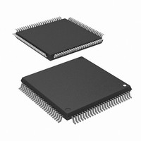
Manufacturer Part Number
R5F2L3A7ANFP#U1
Description
MCU FLASH 48+4KB 64LQFP
Manufacturer
Renesas Electronics America
Series
R8C/Lx/3AAr
Datasheet
1.R5F2L387ANFPU1.pdf
(864 pages)
Specifications of R5F2L3A7ANFP#U1
Core Processor
R8C
Core Size
16/32-Bit
Speed
20MHz
Connectivity
I²C, LIN, SIO, SSU, UART/USART
Peripherals
LCD, POR, PWM, Voltage Detect, WDT
Number Of I /o
88
Program Memory Size
48KB (48K x 8)
Program Memory Type
FLASH
Ram Size
6K x 8
Voltage - Supply (vcc/vdd)
1.8 V ~ 5.5 V
Data Converters
A/D 20x10b; D/A 2x8b
Oscillator Type
Internal
Operating Temperature
-20°C ~ 85°C
Package / Case
64-LQFP
Lead Free Status / RoHS Status
Lead free / RoHS Compliant
Eeprom Size
-
Available stocks
Company
Part Number
Manufacturer
Quantity
Price


R8C/L35A Group, R8C/L36A Group, R8C/L38A Group, R8C/L3AA Group,
R8C/L35B Group, R8C/L36B Group, R8C/L38B Group, R8C/L3AB Group
REJ09B0441-0100 Rev.1.00
Page 663 of 802
Table 32.2
Segment output
Common output
Maximum number of
display pixles
LCD drive timing
Bias control
Table 32.2 lists the Specification Overview of LCD Drive Control Circuit (1) and Table 32.3 lists the Specification
Overview of LCD Drive Control Circuit (2). Figure 32.1 shows a Block Diagram of LCD Drive Control Circuit.
Item
Specification Overview of LCD Drive Control Circuit (1)
The frequency of the internal signal LCDCK for determing the LCD drive timing:
Frame frequency:
Max. 56 pins (SEG0 to SEG55)
• Pins SEG0 to SEG51 can be individually controlled for use as an I/O port or a segment output pin.
• Pins SEG52 to SEG55 can be individually controlled for use as an I/O port or a common
Max. 8 pins (COM0 to COM7)
• The common output pins can be selected.
• Pins COM0 to COM3 can be used I/O ports when not in use as common output pins.
• Pins COM4 to COM7 can be individually controlled for use as an I/O port or a segment
External division resistors or the internal voltage multiplier can be used
(1) When external division resistors are used
• The LCD drive voltage is applied to LCD power supply pins VL1 to VL4 using external
• The following voltage values are applied to LCD power supply pins VL1 to VL4 based on
Note:
The R8C/L35A Group and R8C/L35B Group do not have the VL3 pin, so 1/4 bias cannot
be selected.
(2) When the internal voltage multiplier is used
• 1/4 or 1/2 bias selected:
• 1/3 bias selected:
• The VL1 voltage can be generated internally or input externally.
Note:
The R8C/L35A Group and R8C/L35B Group do not have the VL3 pin, so 1/4 bias and 1/2
bias cannot be selected.
VLCD: LCD power supply voltage
Static
1/2
1/3
1/4
1/8
1/4 bias
1/3 bias
1/2 bias
output/segment output pin.
output pin when not in use as a common output pin.
division resistors.
the bias values set by the LCR0 register.
Based on the VL1 voltage, two times the voltage is generated at the VL2 pin, three times
the voltage at the VL3 pin, and four times the voltage at the VL4 pin.
Based on the VL1 voltage, two times the voltage is generated at pins VL2 and VL3, and
three time the voltage at the VL4 pin.
Bias Value
Oct 30, 2009
Duty
f(LCDCK) =
f(FR) =
COM0
COM0, COM1
COM0 to COM2
COM0 to COM3
COM0 to COM7
VL4 = VLCD
VL3 = 3/4 VLCD
VL2 = 2/4 VLCD
VL1 = 1/4 VLCD
VL4 = VLCD
VL3 = VL2 = 2/3 VLCD
VL1 = 1/3 VLCD
VL4 = VLCD
VL1 = VL2 = VL3 = 1/2 VLCD
Common Pin
f(LCDCK) × duty
Frequency of LCD clock source
2
Voltage Value
n × division ratio
56 dots or 8-segment LCD 7 digits
112 dots or 8-segment LCD 14 digits
168 dots or 8-segment LCD 21 digits
224 dots or 8-segment LCD 28 digits
416 dots or 8-segment LCD 52 digits
Specification
Maximum Number of Display Pixels
32. LCD Drive Control Circuit
Notes:
n = 32 when f32 is selected
n = 4 when fC-LCD is selected
Related parts for R5F2L3A7ANFP#U1
Image
Part Number
Description
Manufacturer
Datasheet
Request
R

Part Number:
Description:
KIT STARTER FOR M16C/29
Manufacturer:
Renesas Electronics America
Datasheet:

Part Number:
Description:
KIT STARTER FOR R8C/2D
Manufacturer:
Renesas Electronics America
Datasheet:

Part Number:
Description:
R0K33062P STARTER KIT
Manufacturer:
Renesas Electronics America
Datasheet:

Part Number:
Description:
KIT STARTER FOR R8C/23 E8A
Manufacturer:
Renesas Electronics America
Datasheet:

Part Number:
Description:
KIT STARTER FOR R8C/25
Manufacturer:
Renesas Electronics America
Datasheet:

Part Number:
Description:
KIT STARTER H8S2456 SHARPE DSPLY
Manufacturer:
Renesas Electronics America
Datasheet:

Part Number:
Description:
KIT STARTER FOR R8C38C
Manufacturer:
Renesas Electronics America
Datasheet:

Part Number:
Description:
KIT STARTER FOR R8C35C
Manufacturer:
Renesas Electronics America
Datasheet:

Part Number:
Description:
KIT STARTER FOR R8CL3AC+LCD APPS
Manufacturer:
Renesas Electronics America
Datasheet:
Part Number:
Description:
KIT STARTER FOR RX610
Manufacturer:
Renesas Electronics America
Datasheet:

Part Number:
Description:
KIT STARTER FOR R32C/118
Manufacturer:
Renesas Electronics America
Datasheet:

Part Number:
Description:
KIT DEV RSK-R8C/26-29
Manufacturer:
Renesas Electronics America
Datasheet:

Part Number:
Description:
KIT STARTER FOR SH7124
Manufacturer:
Renesas Electronics America
Datasheet:

Part Number:
Description:
KIT STARTER FOR H8SX/1622
Manufacturer:
Renesas Electronics America
Datasheet:

Part Number:
Description:
KIT DEV FOR SH7203
Manufacturer:
Renesas Electronics America
Datasheet: