R5F2L3A7ANFP#U1 Renesas Electronics America, R5F2L3A7ANFP#U1 Datasheet - Page 625
R5F2L3A7ANFP#U1
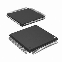
Manufacturer Part Number
R5F2L3A7ANFP#U1
Description
MCU FLASH 48+4KB 64LQFP
Manufacturer
Renesas Electronics America
Series
R8C/Lx/3AAr
Datasheet
1.R5F2L387ANFPU1.pdf
(864 pages)
Specifications of R5F2L3A7ANFP#U1
Core Processor
R8C
Core Size
16/32-Bit
Speed
20MHz
Connectivity
I²C, LIN, SIO, SSU, UART/USART
Peripherals
LCD, POR, PWM, Voltage Detect, WDT
Number Of I /o
88
Program Memory Size
48KB (48K x 8)
Program Memory Type
FLASH
Ram Size
6K x 8
Voltage - Supply (vcc/vdd)
1.8 V ~ 5.5 V
Data Converters
A/D 20x10b; D/A 2x8b
Oscillator Type
Internal
Operating Temperature
-20°C ~ 85°C
Package / Case
64-LQFP
Lead Free Status / RoHS Status
Lead free / RoHS Compliant
Eeprom Size
-
Available stocks
Company
Part Number
Manufacturer
Quantity
Price


R8C/L35A Group, R8C/L36A Group, R8C/L38A Group, R8C/L3AA Group,
R8C/L35B Group, R8C/L36B Group, R8C/L38B Group, R8C/L3AB Group
REJ09B0441-0100 Rev.1.00
Page 588 of 802
27.2.10 IIC bus Status Register (ICSR)
Notes:
1. Each bit is set to 0 by reading 1 before writing 0.
2. This flag is enabled in slave receive mode with the I
3. When two or more master devices attempt to occupy the bus at nearly the same time, if the I
4. The NACKF bit is enabled when the ACKE bit in the ICIER register is set to 1 (when the receive acknowledge bit
5. The RDRF bit is set to 0 when data is read from the ICDRR register.
6. Bits TEND and TDRE are set to 0 when data is written to the ICDRT register.
After Reset
Bit
b0
b1
b2
b3
b4
b5
b6
b7
Address 019Ch
monitors the SDA pin and the data which the I
the bus is occupied by another master.
is set to 1, transfer is halted).
When accessing the ICSR register successively, insert one or more NOP instructions between the instructions
used for access.
Symbol
Symbol
NACKF No acknowledge
Bit
STOP
RDRF
TEND
TDRE
ADZ
AAS
AL
TDRE
b7
0
General call address
recognition flag
Slave address
recognition flag
Arbitration lost flag/
overrun error flag
Stop condition detection flag
detection flag
Receive data register full flag
(1, 5)
Transmit end flag
Transmit data empty flag
TEND
b6
0
Bit Name
Oct 30, 2009
(1, 4)
(1, 2)
(1)
RDRF
(1)
(1, 6)
b5
0
(1, 6)
NACKF
(1)
b4
0
This flag is set to 1 when a general call address is
detected.
This flag is set to 1 when the first frame immediately after
the start condition matches bits SVA0 to SVA6 in the SAR
register in slave receive mode (slave address detection
and general call address detection).
I
This flag indicates that arbitration has been lost
in master mode.
This flag is set to 1
Clock synchronous format:
This flag indicates an overrun error.
This flag is set to 1 when:
This flag is set to 1 when a stop condition is detected
after the frame is transferred.
This flag is set to 1 when no ACKnowledge is detected
from the receive device after transmission.
This flag is set to 1 when receive data is transferred from
registers ICDRS to ICDRR.
I
This flag is set to 1 at the rising edge of the 9th clock cycle
of the SCL signal while the TDRE bit is set to 1.
Clock synchronous format:
This flag is set to 1 when the last bit of the transmit frame
is transmitted.
This flag is set to 1 when:
2
2
2
• The internal SDA signal and SDA pin level do not
• The SDA pin is held high at start condition detection in
• The last bit of the next unit of data is received
• Data is transferred from registers ICDRT to ICDRS and
• The TRS bit in the ICCR1 register is set to 1 (transmit
• A start condition is generated (including retransmission)
• Slave receive mode is changed to slave transmit mode
C bus format:
C bus format:
C bus Interface transmits is different, the AL flag is set to 1 and
match at the rising edge of the SCL signal in master
transmit mode
master transmit/receive mode
while the RDRF bit is set to 1
the CDRT register is empty
mode)
2
C bus format.
STOP
b3
X
(3)
AL
b2
0
when:
Function
AAS
b1
0
ADZ
b0
0
27. I
2
C bus Interface
2
C bus Interface
R/W
R/W
R/W
R/W
R/W
R/W
R/W
R/W
R/W
Related parts for R5F2L3A7ANFP#U1
Image
Part Number
Description
Manufacturer
Datasheet
Request
R

Part Number:
Description:
KIT STARTER FOR M16C/29
Manufacturer:
Renesas Electronics America
Datasheet:

Part Number:
Description:
KIT STARTER FOR R8C/2D
Manufacturer:
Renesas Electronics America
Datasheet:

Part Number:
Description:
R0K33062P STARTER KIT
Manufacturer:
Renesas Electronics America
Datasheet:

Part Number:
Description:
KIT STARTER FOR R8C/23 E8A
Manufacturer:
Renesas Electronics America
Datasheet:

Part Number:
Description:
KIT STARTER FOR R8C/25
Manufacturer:
Renesas Electronics America
Datasheet:

Part Number:
Description:
KIT STARTER H8S2456 SHARPE DSPLY
Manufacturer:
Renesas Electronics America
Datasheet:

Part Number:
Description:
KIT STARTER FOR R8C38C
Manufacturer:
Renesas Electronics America
Datasheet:

Part Number:
Description:
KIT STARTER FOR R8C35C
Manufacturer:
Renesas Electronics America
Datasheet:

Part Number:
Description:
KIT STARTER FOR R8CL3AC+LCD APPS
Manufacturer:
Renesas Electronics America
Datasheet:
Part Number:
Description:
KIT STARTER FOR RX610
Manufacturer:
Renesas Electronics America
Datasheet:

Part Number:
Description:
KIT STARTER FOR R32C/118
Manufacturer:
Renesas Electronics America
Datasheet:

Part Number:
Description:
KIT DEV RSK-R8C/26-29
Manufacturer:
Renesas Electronics America
Datasheet:

Part Number:
Description:
KIT STARTER FOR SH7124
Manufacturer:
Renesas Electronics America
Datasheet:

Part Number:
Description:
KIT STARTER FOR H8SX/1622
Manufacturer:
Renesas Electronics America
Datasheet:

Part Number:
Description:
KIT DEV FOR SH7203
Manufacturer:
Renesas Electronics America
Datasheet: