R5F21346CNFP#U0 Renesas Electronics America, R5F21346CNFP#U0 Datasheet - Page 377
R5F21346CNFP#U0
Manufacturer Part Number
R5F21346CNFP#U0
Description
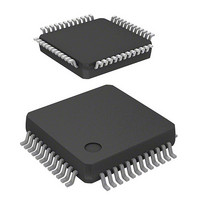
MCU 1KB FLASH 32K ROM 48-LQFP
Manufacturer
Renesas Electronics America
Series
R8C/3x/34Cr
Datasheet
1.R5F21346CNFPU0.pdf
(759 pages)
Specifications of R5F21346CNFP#U0
Core Processor
R8C
Core Size
16/32-Bit
Speed
20MHz
Connectivity
I²C, LIN, SIO, SSU, UART/USART
Peripherals
POR, PWM, Voltage Detect, WDT
Number Of I /o
43
Program Memory Size
32KB (32K x 8)
Program Memory Type
FLASH
Ram Size
2.5K x 8
Voltage - Supply (vcc/vdd)
1.8 V ~ 5.5 V
Data Converters
A/D 12x10b; D/A 2x8b
Oscillator Type
Internal
Operating Temperature
-20°C ~ 85°C
Package / Case
48-LQFP
Lead Free Status / RoHS Status
Lead free / RoHS Compliant
Eeprom Size
-
Available stocks
Company
Part Number
Manufacturer
Quantity
Price


R8C/34C Group
REJ09B0586-0100 Rev.1.00 Jan 13, 2010
Page 344 of 723
Figure 20.12
20.4.21 Changing Output Pins in Registers TRDGRCi (i = 0 or 1) and TRDGRDi
TRDIOC0
TRDIOD0
TRDIOC1
TRDIOD1
TRDIOA0
TRDIOB0
TRDIOA1
TRDIOB1
The TRDGRCi register can be used for output control of the TRDIOAi pin, and the TRDGRDi register can be
used for output control of the TRDIOBi pin. Therefore, each pin output can be controlled as follows:
• TRDIOAi output is controlled by the values in registers TRDGRAi and TRDGRCi.
• TRDIOBi output is controlled by the values in registers TRDGRBi and TRDGRDi.
Change output pins in registers TRDGRCi and TRDGRDi as follows:
• Select 0 (change TRDGRji register output pin) by the IOj3 (j = C or D) bit in the TRDIORCi register.
• Set the BFji bit in the TRDMR register to 0 (general register).
• Set different values in registers TRDGRCi and TRDGRAi. Also, set different values in registers TRDGRDi
Figure 20.13 shows an Operating Example When TRDGRCi Register is Used for Output Control of TRDIOAi
Pin and TRDGRDi Register is Used for Output Control of TRDIOBi Pin.
and TRDGRBi.
Changing Output Pins in Registers TRDGRCi and TRDGRDi
Timer RD0
Timer RD1
Output
control
Output
control
Output
control
Output
control
Output
control
Output
control
Output
control
Output
control
IOC3 = 0 in
TRDIORC0 register
IOC3 = 1
IOD3 = 0 in
TRDIORC0 register
IOD3 = 1
IOC3 = 0 in
TRDIORC1 register
IOC3 = 1
IOD3 = 0 in
TRDIORC1 register
IOD3 = 1
Compare match signal
Compare match signal
Compare match signal
Compare match signal
Compare match signal
Compare match signal
Compare match signal
Compare match signal
Comparator
Comparator
Comparator
Comparator
Comparator
Comparator
Comparator
Comparator
TRDGRC0
TRDGRD0
TRDGRC1
TRDGRD1
TRDGRA0
TRDGRB0
TRDGRA1
TRDGRB1
TRD0
TRD1
20. Timer RD
Related parts for R5F21346CNFP#U0
Image
Part Number
Description
Manufacturer
Datasheet
Request
R

Part Number:
Description:
KIT STARTER FOR M16C/29
Manufacturer:
Renesas Electronics America
Datasheet:

Part Number:
Description:
KIT STARTER FOR R8C/2D
Manufacturer:
Renesas Electronics America
Datasheet:

Part Number:
Description:
R0K33062P STARTER KIT
Manufacturer:
Renesas Electronics America
Datasheet:

Part Number:
Description:
KIT STARTER FOR R8C/23 E8A
Manufacturer:
Renesas Electronics America
Datasheet:

Part Number:
Description:
KIT STARTER FOR R8C/25
Manufacturer:
Renesas Electronics America
Datasheet:

Part Number:
Description:
KIT STARTER H8S2456 SHARPE DSPLY
Manufacturer:
Renesas Electronics America
Datasheet:

Part Number:
Description:
KIT STARTER FOR R8C38C
Manufacturer:
Renesas Electronics America
Datasheet:

Part Number:
Description:
KIT STARTER FOR R8C35C
Manufacturer:
Renesas Electronics America
Datasheet:

Part Number:
Description:
KIT STARTER FOR R8CL3AC+LCD APPS
Manufacturer:
Renesas Electronics America
Datasheet:
Part Number:
Description:
KIT STARTER FOR RX610
Manufacturer:
Renesas Electronics America
Datasheet:

Part Number:
Description:
KIT STARTER FOR R32C/118
Manufacturer:
Renesas Electronics America
Datasheet:

Part Number:
Description:
KIT DEV RSK-R8C/26-29
Manufacturer:
Renesas Electronics America
Datasheet:

Part Number:
Description:
KIT STARTER FOR SH7124
Manufacturer:
Renesas Electronics America
Datasheet:

Part Number:
Description:
KIT STARTER FOR H8SX/1622
Manufacturer:
Renesas Electronics America
Datasheet:

Part Number:
Description:
KIT DEV FOR SH7203
Manufacturer:
Renesas Electronics America
Datasheet: