R5F21346CNFP#U0 Renesas Electronics America, R5F21346CNFP#U0 Datasheet - Page 275
R5F21346CNFP#U0
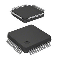
Manufacturer Part Number
R5F21346CNFP#U0
Description
MCU 1KB FLASH 32K ROM 48-LQFP
Manufacturer
Renesas Electronics America
Series
R8C/3x/34Cr
Datasheet
1.R5F21346CNFPU0.pdf
(759 pages)
Specifications of R5F21346CNFP#U0
Core Processor
R8C
Core Size
16/32-Bit
Speed
20MHz
Connectivity
I²C, LIN, SIO, SSU, UART/USART
Peripherals
POR, PWM, Voltage Detect, WDT
Number Of I /o
43
Program Memory Size
32KB (32K x 8)
Program Memory Type
FLASH
Ram Size
2.5K x 8
Voltage - Supply (vcc/vdd)
1.8 V ~ 5.5 V
Data Converters
A/D 12x10b; D/A 2x8b
Oscillator Type
Internal
Operating Temperature
-20°C ~ 85°C
Package / Case
48-LQFP
Lead Free Status / RoHS Status
Lead free / RoHS Compliant
Eeprom Size
-
Available stocks
Company
Part Number
Manufacturer
Quantity
Price


R8C/34C Group
REJ09B0586-0100 Rev.1.00 Jan 13, 2010
Page 242 of 723
18.4
Table 18.3
Notes:
Count sources
Count operations
Width and period of
output waveform
Count start condition
Count stop conditions
Interrupt request
generation timing
TRBO pin function
INT0 pin function
Read from timer
Write to timer
Selectable functions
In programmable waveform generation mode, the signal output from the TRBO pin is inverted each time the
counter underflows, while the values in registers TRBPR and TRBSC are counted alternately (refer to Table 18.3
Programmable Waveform Generation Mode Specifications). Counting starts by counting the setting value in the
TRBPR register. The TRBOCR register is unused in this mode.
Figure 18.3 shows an Operating Example of Timer RB in Programmable Waveform Generation Mode.
1. Even when counting the secondary period, the TRBPR register may be read.
2. The set values are reflected in the waveform output beginning with the following primary period after writing to
3. The value written to the TOCNT bit is enabled by the following.
the TRBPR register.
• When counting starts.
• When a timer RB interrupt request is generated.
Programmable Waveform Generation Mode
The contents after the TOCNT bit is changed are reflected from the output of the following primary period.
Item
Programmable Waveform Generation Mode Specifications
f1, f2, f8, timer RA underflow
• Decrement
• When the timer underflows, it reloads the contents of the primary reload and secondary
Primary period: (n+1)(m+1)/fi
Secondary period: (n+1)(p+1)/fi
Period: (n+1){(m+1)+(p+1)}/fi
fi: Count source frequency
n: Value set in TRBPRE register
p: Value set in TRBSC register
1 (count start) is written to the TSTART bit in the TRBCR register.
• 0 (count stop) is written to the TSTART bit in the TRBCR register.
• 1 (count forcibly stop) is written to the TSTOP bit in the TRBCR register.
In half a cycle of the count source, after timer RB underflows during the secondary period
(at the same time as the TRBO output change) [timer RB interrupt]
Programmable output port or pulse output
Programmable I/O port or INT0 interrupt input
The count value can be read out by reading registers TRBPR and TRBPRE
• When registers TRBPRE, TRBSC, and TRBPR are written while the count is stopped,
• When registers TRBPRE, TRBSC, and TRBPR are written to during count operation,
• Output level select function
• TRBO pin output switch function
reload registers alternately before the count continues.
values are written to both the reload register and counter.
values are written to the reload registers only.
The output level during primary and secondary periods is selected by the TOPL bit in the
TRBIOC register.
Timer RB pulse output or P3_1 (P1_3) latch output is selected by the TOCNT bit in the
TRBIOC register.
(3)
m: Value set in TRBPR register
Specification
(2)
(1)
.
18. Timer RB
Related parts for R5F21346CNFP#U0
Image
Part Number
Description
Manufacturer
Datasheet
Request
R

Part Number:
Description:
KIT STARTER FOR M16C/29
Manufacturer:
Renesas Electronics America
Datasheet:

Part Number:
Description:
KIT STARTER FOR R8C/2D
Manufacturer:
Renesas Electronics America
Datasheet:

Part Number:
Description:
R0K33062P STARTER KIT
Manufacturer:
Renesas Electronics America
Datasheet:

Part Number:
Description:
KIT STARTER FOR R8C/23 E8A
Manufacturer:
Renesas Electronics America
Datasheet:

Part Number:
Description:
KIT STARTER FOR R8C/25
Manufacturer:
Renesas Electronics America
Datasheet:

Part Number:
Description:
KIT STARTER H8S2456 SHARPE DSPLY
Manufacturer:
Renesas Electronics America
Datasheet:

Part Number:
Description:
KIT STARTER FOR R8C38C
Manufacturer:
Renesas Electronics America
Datasheet:

Part Number:
Description:
KIT STARTER FOR R8C35C
Manufacturer:
Renesas Electronics America
Datasheet:

Part Number:
Description:
KIT STARTER FOR R8CL3AC+LCD APPS
Manufacturer:
Renesas Electronics America
Datasheet:
Part Number:
Description:
KIT STARTER FOR RX610
Manufacturer:
Renesas Electronics America
Datasheet:

Part Number:
Description:
KIT STARTER FOR R32C/118
Manufacturer:
Renesas Electronics America
Datasheet:

Part Number:
Description:
KIT DEV RSK-R8C/26-29
Manufacturer:
Renesas Electronics America
Datasheet:

Part Number:
Description:
KIT STARTER FOR SH7124
Manufacturer:
Renesas Electronics America
Datasheet:

Part Number:
Description:
KIT STARTER FOR H8SX/1622
Manufacturer:
Renesas Electronics America
Datasheet:

Part Number:
Description:
KIT DEV FOR SH7203
Manufacturer:
Renesas Electronics America
Datasheet: