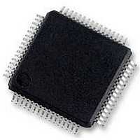
S9S12HY64J0MLH Freescale Semiconductor, S9S12HY64J0MLH Datasheet - Page 502

S9S12HY64J0MLH
Manufacturer Part Number
S9S12HY64J0MLH
Description
MCU 64K FLASH AUTO 64-LQFP
Manufacturer
Freescale Semiconductor
Series
HCS12r
Datasheet
1.S9S12HA32J0CLL.pdf
(792 pages)
Specifications of S9S12HY64J0MLH
Core Processor
HCS12
Core Size
16-Bit
Speed
32MHz
Connectivity
CAN, EBI/EMI, I²C, IrDA, LIN, SCI, SPI
Peripherals
LCD, Motor control PWM, POR, PWM, WDT
Number Of I /o
50
Program Memory Size
64KB (64K x 8)
Program Memory Type
FLASH
Eeprom Size
4K x 8
Ram Size
4K x 8
Voltage - Supply (vcc/vdd)
4.5 V ~ 5.5 V
Data Converters
A/D 6x10b
Oscillator Type
Internal
Operating Temperature
-40°C ~ 125°C
Package / Case
64-LQFP
Controller Family/series
S12
No. Of I/o's
50
Ram Memory Size
4KB
Cpu Speed
64MHz
No. Of Timers
2
Rohs Compliant
Yes
Processor Series
S12HY
Core
HCS12
3rd Party Development Tools
EWHCS12
Development Tools By Supplier
DEMO9S12HY64
Lead Free Status / RoHS Status
Lead free / RoHS Compliant
Available stocks
Company
Part Number
Manufacturer
Quantity
Price
Company:
Part Number:
S9S12HY64J0MLH
Manufacturer:
Freescale Semiconductor
Quantity:
10 000
- Current page: 502 of 792
- Download datasheet (4Mb)
Module Base + 0x0010 = TC0H
Module Base + 0x0011 = TC0L
Timer Module (TIM16B8CV2) Block Description
14.3.2.14 Timer Input Capture/Output Compare Registers High and Low 0–7
Depending on the TIOS bit for the corresponding channel, these registers are used to latch the value of the
free-running counter when a defined transition is sensed by the corresponding input capture edge detector
or to trigger an output action for output compare.
Read: Anytime
Write: Anytime for output compare function.Writes to these registers have no meaning or effect during
input capture. All timer input capture/output compare registers are reset to 0x0000.
502
Field
TOF
7
Reset
Reset
W
W
R
R
Timer Overflow Flag — Set when 16-bit free-running timer overflows from 0xFFFF to 0x0000. Clearing this bit
requires writing a one to bit 7 of TFLG2 register while the TEN bit of TSCR1 or PAEN bit of PACTL is set to one
(See also TCRE control bit explanation.)
0x0012 = TC1H
0x0014 = TC2H
0x0016 = TC3H
0x0013 = TC1L
0x0015 = TC2L
0x0017 = TC3L
(TCxH and TCxL)
Read/Write access in byte mode for high byte should takes place before low
byte otherwise it will give a different result.
Figure 14-22. Timer Input Capture/Output Compare Register x High (TCxH)
Figure 14-23. Timer Input Capture/Output Compare Register x Low (TCxL)
Bit 15
Bit 7
15
0
0
7
Bit 14
Bit 6
14
0
0
6
MC9S12HY/HA-Family Reference Manual, Rev. 1.04
Table 14-17. TRLG2 Field Descriptions
0x0018 = TC4H
0x001A = TC5H
0x001C = TC6H
0x001E = TC7H
0x0019 = TC4L
0x001B = TC5L
0x001D = TC6L
0x001F = TC7L
Bit 13
Bit 5
13
0
0
5
NOTE
Bit 12
Bit 4
12
0
0
4
Description
Bit 11
Bit 3
11
0
0
3
Bit 10
Bit 2
10
0
0
2
Freescale Semiconductor
Bit 9
Bit 1
0
0
9
1
Bit 8
Bit 0
0
0
0
0
Related parts for S9S12HY64J0MLH
Image
Part Number
Description
Manufacturer
Datasheet
Request
R
Part Number:
Description:
Manufacturer:
Freescale Semiconductor, Inc
Datasheet:
Part Number:
Description:
Manufacturer:
Freescale Semiconductor, Inc
Datasheet:
Part Number:
Description:
Manufacturer:
Freescale Semiconductor, Inc
Datasheet:
Part Number:
Description:
Manufacturer:
Freescale Semiconductor, Inc
Datasheet:
Part Number:
Description:
Manufacturer:
Freescale Semiconductor, Inc
Datasheet:
Part Number:
Description:
Manufacturer:
Freescale Semiconductor, Inc
Datasheet:
Part Number:
Description:
Manufacturer:
Freescale Semiconductor, Inc
Datasheet:
Part Number:
Description:
Manufacturer:
Freescale Semiconductor, Inc
Datasheet:
Part Number:
Description:
Manufacturer:
Freescale Semiconductor, Inc
Datasheet:
Part Number:
Description:
Manufacturer:
Freescale Semiconductor, Inc
Datasheet:
Part Number:
Description:
Manufacturer:
Freescale Semiconductor, Inc
Datasheet:
Part Number:
Description:
Manufacturer:
Freescale Semiconductor, Inc
Datasheet:
Part Number:
Description:
Manufacturer:
Freescale Semiconductor, Inc
Datasheet:
Part Number:
Description:
Manufacturer:
Freescale Semiconductor, Inc
Datasheet:
Part Number:
Description:
Manufacturer:
Freescale Semiconductor, Inc
Datasheet:


