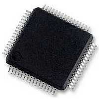
S9S12HY64J0MLH Freescale Semiconductor, S9S12HY64J0MLH Datasheet - Page 121

S9S12HY64J0MLH
Manufacturer Part Number
S9S12HY64J0MLH
Description
MCU 64K FLASH AUTO 64-LQFP
Manufacturer
Freescale Semiconductor
Series
HCS12r
Datasheet
1.S9S12HA32J0CLL.pdf
(792 pages)
Specifications of S9S12HY64J0MLH
Core Processor
HCS12
Core Size
16-Bit
Speed
32MHz
Connectivity
CAN, EBI/EMI, I²C, IrDA, LIN, SCI, SPI
Peripherals
LCD, Motor control PWM, POR, PWM, WDT
Number Of I /o
50
Program Memory Size
64KB (64K x 8)
Program Memory Type
FLASH
Eeprom Size
4K x 8
Ram Size
4K x 8
Voltage - Supply (vcc/vdd)
4.5 V ~ 5.5 V
Data Converters
A/D 6x10b
Oscillator Type
Internal
Operating Temperature
-40°C ~ 125°C
Package / Case
64-LQFP
Controller Family/series
S12
No. Of I/o's
50
Ram Memory Size
4KB
Cpu Speed
64MHz
No. Of Timers
2
Rohs Compliant
Yes
Processor Series
S12HY
Core
HCS12
3rd Party Development Tools
EWHCS12
Development Tools By Supplier
DEMO9S12HY64
Lead Free Status / RoHS Status
Lead free / RoHS Compliant
Available stocks
Company
Part Number
Manufacturer
Quantity
Price
Company:
Part Number:
S9S12HY64J0MLH
Manufacturer:
Freescale Semiconductor
Quantity:
10 000
- Current page: 121 of 792
- Download datasheet (4Mb)
1
2
2.3.81
Freescale Semiconductor
Function
Address 0x0298
Read: Anytime.
Write: Anytime
Special SPI/PWM&IIC priority
Altern.
Field
Reset
PTV
PTV
6, 4
7,5
W
R
Port V general purpose input/output data—Data Register, Motor driver PWM output
Port V pins are associated with the Motor PWM output.
When not used with the alternative functions, these pins can be used as general purpose I/O. If the associated data
direction bits of these pins are set to 1, a read returns the value of the port register, otherwise the buffered pin input
state is read.
Port V general purpose input/output data—Data Register, Motor driver PWM output, TIM1 channel 3,2
Port V pins are associated with the Motor PWM output and TIM1 channels 3-2
When not used with the alternative functions, these pins can be used as general purpose I/O. If the associated data
direction bits of these pins are set to 1, a read returns the value of the port register, otherwise the buffered pin input
state is read.
M3C1P
• The Motor driver PWM takes precedence over the general purpose I/O function.
• The Motor driver PWM takes precedence over the TIM1 and the general purpose I/O function.
• The TIM1 output compare function takes precedence over the general purpose I/O function if the related channels
PTV7
Port V Data Register (PTV)
is enabled
—
—
—
—
0
7
1
IOC1_3
M3C1M
PTV6
—
—
—
0
6
MC9S12HY/HA-Family Reference Manual, Rev. 1.04
Table 2-68. PTV register Field Descriptions
Figure 2-79. Port V Data Register (PTV)
M3C0P
PTV5
—
—
—
—
0
5
M3C0M
IOC1_2
PTV4
—
—
—
0
4
Description
M2C1P
PWM7
PTV3
SDA
SS
—
3
0
M2C1M
IOC1_1
PWM6
PTV2
SCK
—
Port Integration Module (S12HYPIMV1)
0
2
M2C0P
Access: User read/write
PWM5
MOSI
PTV1
—
—
0
1
IOC1_0
M2C0M
MISO
PWM4
PTV0
SCL
0
0
2
121
1
Related parts for S9S12HY64J0MLH
Image
Part Number
Description
Manufacturer
Datasheet
Request
R
Part Number:
Description:
Manufacturer:
Freescale Semiconductor, Inc
Datasheet:
Part Number:
Description:
Manufacturer:
Freescale Semiconductor, Inc
Datasheet:
Part Number:
Description:
Manufacturer:
Freescale Semiconductor, Inc
Datasheet:
Part Number:
Description:
Manufacturer:
Freescale Semiconductor, Inc
Datasheet:
Part Number:
Description:
Manufacturer:
Freescale Semiconductor, Inc
Datasheet:
Part Number:
Description:
Manufacturer:
Freescale Semiconductor, Inc
Datasheet:
Part Number:
Description:
Manufacturer:
Freescale Semiconductor, Inc
Datasheet:
Part Number:
Description:
Manufacturer:
Freescale Semiconductor, Inc
Datasheet:
Part Number:
Description:
Manufacturer:
Freescale Semiconductor, Inc
Datasheet:
Part Number:
Description:
Manufacturer:
Freescale Semiconductor, Inc
Datasheet:
Part Number:
Description:
Manufacturer:
Freescale Semiconductor, Inc
Datasheet:
Part Number:
Description:
Manufacturer:
Freescale Semiconductor, Inc
Datasheet:
Part Number:
Description:
Manufacturer:
Freescale Semiconductor, Inc
Datasheet:
Part Number:
Description:
Manufacturer:
Freescale Semiconductor, Inc
Datasheet:
Part Number:
Description:
Manufacturer:
Freescale Semiconductor, Inc
Datasheet:


