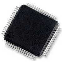
S9S12HY64J0MLH Freescale Semiconductor, S9S12HY64J0MLH Datasheet - Page 478

S9S12HY64J0MLH
Manufacturer Part Number
S9S12HY64J0MLH
Description
MCU 64K FLASH AUTO 64-LQFP
Manufacturer
Freescale Semiconductor
Series
HCS12r
Datasheet
1.S9S12HA32J0CLL.pdf
(792 pages)
Specifications of S9S12HY64J0MLH
Core Processor
HCS12
Core Size
16-Bit
Speed
32MHz
Connectivity
CAN, EBI/EMI, I²C, IrDA, LIN, SCI, SPI
Peripherals
LCD, Motor control PWM, POR, PWM, WDT
Number Of I /o
50
Program Memory Size
64KB (64K x 8)
Program Memory Type
FLASH
Eeprom Size
4K x 8
Ram Size
4K x 8
Voltage - Supply (vcc/vdd)
4.5 V ~ 5.5 V
Data Converters
A/D 6x10b
Oscillator Type
Internal
Operating Temperature
-40°C ~ 125°C
Package / Case
64-LQFP
Controller Family/series
S12
No. Of I/o's
50
Ram Memory Size
4KB
Cpu Speed
64MHz
No. Of Timers
2
Rohs Compliant
Yes
Processor Series
S12HY
Core
HCS12
3rd Party Development Tools
EWHCS12
Development Tools By Supplier
DEMO9S12HY64
Lead Free Status / RoHS Status
Lead free / RoHS Compliant
Available stocks
Company
Part Number
Manufacturer
Quantity
Price
Company:
Part Number:
S9S12HY64J0MLH
Manufacturer:
Freescale Semiconductor
Quantity:
10 000
- Current page: 478 of 792
- Download datasheet (4Mb)
Serial Peripheral Interface (S12SPIV5)
When the third edge occurs, the value previously latched from the serial data input pin is shifted into the
LSB or MSB of the SPI shift register, depending on LSBFE bit. After this edge, the next bit of the master
data is coupled out of the serial data output pin of the master to the serial input pin on the slave.
This process continues for a total of n
edges and shifting taking place on odd numbered edges.
Data reception is double buffered, data is serially shifted into the SPI shift register during the transfer and
is transferred to the parallel SPI data register after the last bit is shifted in.
After 2n
Figure 13-14
slave timing diagram because the SCK, MISO, and MOSI pins are connected directly between the master
and the slave. The MISO signal is the output from the slave, and the MOSI signal is the output from the
master. The SS line is the slave select input to the slave. The SS pin of the master must be either high or
reconfigured as a general-purpose output not affecting the SPI.
478
•
•
End of Idle State
SCK Edge Number
SCK (CPOL = 0)
SCK (CPOL = 1)
SAMPLE I
MOSI/MISO
CHANGE O
CHANGE O
SEL SS (O)
Master only
SEL SS (I)
MOSI pin
MISO pin
Data that was previously in the SPI data register of the master is now in the data register of the
slave, and data that was in the data register of the slave is in the master.
The SPIF flag bit in SPISR is set indicating that the transfer is complete.
Figure 13-14. SPI Clock Format 1 (CPHA = 1), with 8-Bit Transfer Width selected (XFRW = 0)
MSB first (LSBFE = 0):
t
t
t
LSB first (LSBFE = 1):
L
T
I
1
= Minimum idling time between transfers (minimum SS high time), not required for back-to-back transfers
= Minimum leading time before the first SCK edge, not required for back-to-back transfers
= Minimum trailing time after the last SCK edge
SCK edges:
shows two clocking variations for CPHA = 1. The diagram may be interpreted as a master or
t
L
1
MSB
LSB
2
MC9S12HY/HA-Family Reference Manual, Rev. 1.04
3
Begin
Bit 6
Bit 1
4
1
edges on the SCK line with data being latched on even numbered
5
Bit 5
Bit 2
6
7
Bit 4
Bit 3
8
Transfer
9
Bit 3
Bit 4
10
11
Bit 2
Bit 5
12
13 14
Bit 1
Bit 6
End
15
MSB
LSB
16
t
T
Minimum 1/2 SCK
Freescale Semiconductor
Begin of Idle State
t
I
for t
T
t
, t
L
l
, t
L
Related parts for S9S12HY64J0MLH
Image
Part Number
Description
Manufacturer
Datasheet
Request
R
Part Number:
Description:
Manufacturer:
Freescale Semiconductor, Inc
Datasheet:
Part Number:
Description:
Manufacturer:
Freescale Semiconductor, Inc
Datasheet:
Part Number:
Description:
Manufacturer:
Freescale Semiconductor, Inc
Datasheet:
Part Number:
Description:
Manufacturer:
Freescale Semiconductor, Inc
Datasheet:
Part Number:
Description:
Manufacturer:
Freescale Semiconductor, Inc
Datasheet:
Part Number:
Description:
Manufacturer:
Freescale Semiconductor, Inc
Datasheet:
Part Number:
Description:
Manufacturer:
Freescale Semiconductor, Inc
Datasheet:
Part Number:
Description:
Manufacturer:
Freescale Semiconductor, Inc
Datasheet:
Part Number:
Description:
Manufacturer:
Freescale Semiconductor, Inc
Datasheet:
Part Number:
Description:
Manufacturer:
Freescale Semiconductor, Inc
Datasheet:
Part Number:
Description:
Manufacturer:
Freescale Semiconductor, Inc
Datasheet:
Part Number:
Description:
Manufacturer:
Freescale Semiconductor, Inc
Datasheet:
Part Number:
Description:
Manufacturer:
Freescale Semiconductor, Inc
Datasheet:
Part Number:
Description:
Manufacturer:
Freescale Semiconductor, Inc
Datasheet:
Part Number:
Description:
Manufacturer:
Freescale Semiconductor, Inc
Datasheet:


