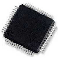
S9S12HY64J0MLH Freescale Semiconductor, S9S12HY64J0MLH Datasheet - Page 490

S9S12HY64J0MLH
Manufacturer Part Number
S9S12HY64J0MLH
Description
MCU 64K FLASH AUTO 64-LQFP
Manufacturer
Freescale Semiconductor
Series
HCS12r
Datasheet
1.S9S12HA32J0CLL.pdf
(792 pages)
Specifications of S9S12HY64J0MLH
Core Processor
HCS12
Core Size
16-Bit
Speed
32MHz
Connectivity
CAN, EBI/EMI, I²C, IrDA, LIN, SCI, SPI
Peripherals
LCD, Motor control PWM, POR, PWM, WDT
Number Of I /o
50
Program Memory Size
64KB (64K x 8)
Program Memory Type
FLASH
Eeprom Size
4K x 8
Ram Size
4K x 8
Voltage - Supply (vcc/vdd)
4.5 V ~ 5.5 V
Data Converters
A/D 6x10b
Oscillator Type
Internal
Operating Temperature
-40°C ~ 125°C
Package / Case
64-LQFP
Controller Family/series
S12
No. Of I/o's
50
Ram Memory Size
4KB
Cpu Speed
64MHz
No. Of Timers
2
Rohs Compliant
Yes
Processor Series
S12HY
Core
HCS12
3rd Party Development Tools
EWHCS12
Development Tools By Supplier
DEMO9S12HY64
Lead Free Status / RoHS Status
Lead free / RoHS Compliant
Available stocks
Company
Part Number
Manufacturer
Quantity
Price
Company:
Part Number:
S9S12HY64J0MLH
Manufacturer:
Freescale Semiconductor
Quantity:
10 000
- Current page: 490 of 792
- Download datasheet (4Mb)
Timer Module (TIM16B8CV2) Block Description
14.2.7
This pin serves as input capture or output compare for channel 1.
14.2.8
This pin serves as input capture or output compare for channel 0.
14.3
This section provides a detailed description of all memory and registers.
14.3.1
The memory map for the TIM16B8CV2 module is given below in
register is the address offset. The total address for each register is the sum of the base address for the
TIM16B8CV2 module and the address offset for each register.
14.3.2
490
This section consists of register descriptions in address order. Each description includes a standard
register diagram with an associated figure number. Details of register bit and field function follow the
register diagrams, in bit order.
Register
CFORC
TCNTH
0x0000
0x0001
0x0002
0x0003
0x0004
0x0005
TCNTL
OC7M
Name
OC7D
TIOS
Memory Map and Register Definition
IOC1 — Input Capture and Output Compare Channel 1 Pin
IOC0 — Input Capture and Output Compare Channel 0 Pin
Module Memory Map
Register Descriptions
For the description of interrupts see
W
W
W
W
W
W
R
R
R
R
R
R
TCNT15
Figure 14-5. TIM16B8CV2 Register Summary (Sheet 1 of 3)
OC7M7
OC7D7
TCNT7
FOC7
IOS7
Bit 7
0
MC9S12HY/HA-Family Reference Manual, Rev. 1.04
= Unimplemented or Reserved
TCNT14
OC7M6
OC7D6
TCNT6
FOC6
IOS6
6
0
TCNT13
OC7M5
OC7D5
TCNT5
FOC5
IOS5
5
0
NOTE
Section 14.6,
TCNT12
OC7M4
OC7D4
TCNT4
FOC4
IOS4
4
0
TCNT11
OC7M3
OC7D3
TCNT3
FOC3
IOS3
Figure
“Interrupts”.
3
0
14-5. The address listed for each
TCNT10
OC7M2
OC7D2
TCNT2
FOC2
IOS2
2
0
OC7M1
Freescale Semiconductor
OC7D1
TCNT9
TCNT1
FOC1
IOS1
1
0
OC7M0
OC7D0
TCNT8
TCNT0
FOC0
IOS0
Bit 0
0
Related parts for S9S12HY64J0MLH
Image
Part Number
Description
Manufacturer
Datasheet
Request
R
Part Number:
Description:
Manufacturer:
Freescale Semiconductor, Inc
Datasheet:
Part Number:
Description:
Manufacturer:
Freescale Semiconductor, Inc
Datasheet:
Part Number:
Description:
Manufacturer:
Freescale Semiconductor, Inc
Datasheet:
Part Number:
Description:
Manufacturer:
Freescale Semiconductor, Inc
Datasheet:
Part Number:
Description:
Manufacturer:
Freescale Semiconductor, Inc
Datasheet:
Part Number:
Description:
Manufacturer:
Freescale Semiconductor, Inc
Datasheet:
Part Number:
Description:
Manufacturer:
Freescale Semiconductor, Inc
Datasheet:
Part Number:
Description:
Manufacturer:
Freescale Semiconductor, Inc
Datasheet:
Part Number:
Description:
Manufacturer:
Freescale Semiconductor, Inc
Datasheet:
Part Number:
Description:
Manufacturer:
Freescale Semiconductor, Inc
Datasheet:
Part Number:
Description:
Manufacturer:
Freescale Semiconductor, Inc
Datasheet:
Part Number:
Description:
Manufacturer:
Freescale Semiconductor, Inc
Datasheet:
Part Number:
Description:
Manufacturer:
Freescale Semiconductor, Inc
Datasheet:
Part Number:
Description:
Manufacturer:
Freescale Semiconductor, Inc
Datasheet:
Part Number:
Description:
Manufacturer:
Freescale Semiconductor, Inc
Datasheet:


