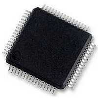
S9S12HY64J0MLH Freescale Semiconductor, S9S12HY64J0MLH Datasheet - Page 129

S9S12HY64J0MLH
Manufacturer Part Number
S9S12HY64J0MLH
Description
MCU 64K FLASH AUTO 64-LQFP
Manufacturer
Freescale Semiconductor
Series
HCS12r
Datasheet
1.S9S12HA32J0CLL.pdf
(792 pages)
Specifications of S9S12HY64J0MLH
Core Processor
HCS12
Core Size
16-Bit
Speed
32MHz
Connectivity
CAN, EBI/EMI, I²C, IrDA, LIN, SCI, SPI
Peripherals
LCD, Motor control PWM, POR, PWM, WDT
Number Of I /o
50
Program Memory Size
64KB (64K x 8)
Program Memory Type
FLASH
Eeprom Size
4K x 8
Ram Size
4K x 8
Voltage - Supply (vcc/vdd)
4.5 V ~ 5.5 V
Data Converters
A/D 6x10b
Oscillator Type
Internal
Operating Temperature
-40°C ~ 125°C
Package / Case
64-LQFP
Controller Family/series
S12
No. Of I/o's
50
Ram Memory Size
4KB
Cpu Speed
64MHz
No. Of Timers
2
Rohs Compliant
Yes
Processor Series
S12HY
Core
HCS12
3rd Party Development Tools
EWHCS12
Development Tools By Supplier
DEMO9S12HY64
Lead Free Status / RoHS Status
Lead free / RoHS Compliant
Available stocks
Company
Part Number
Manufacturer
Quantity
Price
Company:
Part Number:
S9S12HY64J0MLH
Manufacturer:
Freescale Semiconductor
Quantity:
10 000
- Current page: 129 of 792
- Download datasheet (4Mb)
2.4.2.4
If the pin is used as an output this register allows the configuration of the drive strength independent of the
use with a peripheral module.
2.4.2.5
This register turns on a pull-up or pull-down device on the related pins determined by the associated
polarity select register (2.4.2.6/2-129).
The pull device becomes active only if the pin is used as an input or as a wired-or output. Some peripheral
module only allow certain configurations of pull devices to become active. Refer to the respective bit
descriptions.
2.4.2.6
This register selects either a pull-up or pull-down device if enabled.
It becomes only active if the pin is used as an input. A pull-up device can be activated if the pin is used as
a wired-or output.
Freescale Semiconductor
Reduced drive register (RDRx)
Pull device enable register (PERx)
Polarity select register (PPSx)
Due to internal synchronization circuits, it can take up to 2 bus clock cycles
until the correct value is read on port data or port input registers, when
changing the data direction register.
Module
Figure 2-87. Illustration of I/O pin functionality
MC9S12HY/HA-Family Reference Manual, Rev. 1.04
DDR
PTI
PT
data out
output enable
module enable
0
1
1
1
NOTE
0
0
PIN
Port Integration Module (S12HYPIMV1)
129
Related parts for S9S12HY64J0MLH
Image
Part Number
Description
Manufacturer
Datasheet
Request
R
Part Number:
Description:
Manufacturer:
Freescale Semiconductor, Inc
Datasheet:
Part Number:
Description:
Manufacturer:
Freescale Semiconductor, Inc
Datasheet:
Part Number:
Description:
Manufacturer:
Freescale Semiconductor, Inc
Datasheet:
Part Number:
Description:
Manufacturer:
Freescale Semiconductor, Inc
Datasheet:
Part Number:
Description:
Manufacturer:
Freescale Semiconductor, Inc
Datasheet:
Part Number:
Description:
Manufacturer:
Freescale Semiconductor, Inc
Datasheet:
Part Number:
Description:
Manufacturer:
Freescale Semiconductor, Inc
Datasheet:
Part Number:
Description:
Manufacturer:
Freescale Semiconductor, Inc
Datasheet:
Part Number:
Description:
Manufacturer:
Freescale Semiconductor, Inc
Datasheet:
Part Number:
Description:
Manufacturer:
Freescale Semiconductor, Inc
Datasheet:
Part Number:
Description:
Manufacturer:
Freescale Semiconductor, Inc
Datasheet:
Part Number:
Description:
Manufacturer:
Freescale Semiconductor, Inc
Datasheet:
Part Number:
Description:
Manufacturer:
Freescale Semiconductor, Inc
Datasheet:
Part Number:
Description:
Manufacturer:
Freescale Semiconductor, Inc
Datasheet:
Part Number:
Description:
Manufacturer:
Freescale Semiconductor, Inc
Datasheet:


