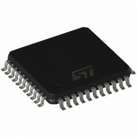
ST72F324J6T6 STMicroelectronics, ST72F324J6T6 Datasheet - Page 185

ST72F324J6T6
Manufacturer Part Number
ST72F324J6T6
Description
IC MCU 8BIT 32K 44-TQFP
Manufacturer
STMicroelectronics
Series
ST7r
Specifications of ST72F324J6T6
Core Processor
ST7
Core Size
8-Bit
Speed
8MHz
Connectivity
SCI, SPI
Peripherals
LVD, POR, PWM, WDT
Number Of I /o
32
Program Memory Size
32KB (32K x 8)
Program Memory Type
FLASH
Ram Size
1K x 8
Voltage - Supply (vcc/vdd)
3.8 V ~ 5.5 V
Data Converters
A/D 12x10b
Oscillator Type
Internal
Operating Temperature
-40°C ~ 85°C
Package / Case
44-TQFP, 44-VQFP
Controller Family/series
ST7
No. Of I/o's
32
Ram Memory Size
1KB
Cpu Speed
8MHz
No. Of Timers
2
Embedded Interface Type
SCI, SPI
No. Of Pwm Channels
1
Rohs Compliant
Yes
Processor Series
ST72F3x
Core
ST7
Data Bus Width
8 bit
Data Ram Size
1024 B
Interface Type
SCI, SPI
Maximum Clock Frequency
8 MHz
Number Of Programmable I/os
32
Number Of Timers
4 bit
Operating Supply Voltage
3.8 V to 5.5 V
Maximum Operating Temperature
+ 85 C
Mounting Style
SMD/SMT
Development Tools By Supplier
ST7F521-IND/USB, ST7232X-EVAL, ST7MDT20-DVP3, ST7MDT20J-EMU3, STX-RLINK
Minimum Operating Temperature
- 40 C
On-chip Adc
10 bit
Cpu Family
ST7
Device Core Size
8b
Frequency (max)
8MHz
Total Internal Ram Size
1KB
# I/os (max)
32
Number Of Timers - General Purpose
2
Operating Supply Voltage (typ)
5V
Operating Supply Voltage (max)
5.5V
Operating Supply Voltage (min)
3.8V
Instruction Set Architecture
CISC
Operating Temp Range
-40C to 85C
Operating Temperature Classification
Industrial
Mounting
Surface Mount
Pin Count
44
Package Type
TQFP
For Use With
497-8222 - UPS (LINE INTERACTIVE - 450W)497-8436 - BOARD EVAL UPS 450W VOUT=220V497-6421 - BOARD EVAL DGTL BATT CHGR DESIGN
Lead Free Status / RoHS Status
Contains lead / RoHS non-compliant
Eeprom Size
-
Lead Free Status / Rohs Status
In Transition
Other names
497-2108
Available stocks
Company
Part Number
Manufacturer
Quantity
Price
Company:
Part Number:
ST72F324J6T6
Manufacturer:
STMicroelectronics
Quantity:
10 000
Part Number:
ST72F324J6T6
Manufacturer:
ST
Quantity:
20 000
Company:
Part Number:
ST72F324J6T6/TR
Manufacturer:
STMicroelectronics
Quantity:
10 000
ST72324Bxx
15
15.1
15.1.1
15.1.2
Known limitations
All Flash and ROM devices
Safe connection of OSC1/OSC2 pins
The OSC1 and/or OSC2 pins must not be left unconnected, otherwise the ST7 main
oscillator may start and, in this configuration, could generate an f
excess of the allowed maximum (> 16 MHz), putting the ST7 in an unsafe/undefined state.
Refer to
External interrupt missed
To avoid any risk of generating a parasitic interrupt, the edge detector is automatically
disabled for one clock cycle during an access to either DDR and OR. Any input signal edge
during this period will not be detected and will not generate an interrupt.
This case can typically occur if the application refreshes the port configuration registers at
intervals during runtime.
Workaround
The workaround is based on software checking the level on the interrupt pin before and after
writing to the PxOR or PxDDR registers. If there is a level change (depending on the
sensitivity programmed for this pin) the interrupt routine is invoked using the call instruction
with three extra PUSH instructions before executing the interrupt routine (this is to make the
call compatible with the IRET instruction at the end of the interrupt service routine).
But detection of the level change does not make sure that edge occurs during the critical
one cycle duration and the interrupt has been missed. This may lead to occurrence of same
interrupt twice (one hardware and another with software call).
To avoid this, a semaphore is set to ‘1’ before checking the level change. The semaphore is
changed to level '0' inside the interrupt routine. When a level change is detected, the
semaphore status is checked and if it is ‘1’ this means that the last interrupt has been
missed. In this case, the interrupt routine is invoked with the call instruction.
There is another possible case that is, if writing to PxOR or PxDDR is done with global
interrupts disabled (interrupt mask bit set). In this case, the semaphore is changed to ‘1’
when the level change is detected. Detecting a missed interrupt is done after the global
interrupts are enabled (interrupt mask bit reset) and by checking the status of the
semaphore. If it is ‘1’ this means that the last interrupt was missed and the interrupt routine
is invoked with the call instruction.
To implement the workaround, the following software sequence is to be followed for writing
into the PxOR/PxDDR registers. The example is for Port PF1 with falling edge interrupt
sensitivity. The software sequence is given for both cases (global interrupt
disabled/enabled).
Section 6.3 on page
32.
OSC
clock frequency in
Known limitations
185/193


