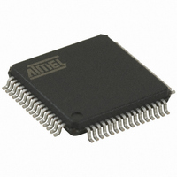
AT32UC3B0512-A2UT Atmel, AT32UC3B0512-A2UT Datasheet - Page 616

AT32UC3B0512-A2UT
Manufacturer Part Number
AT32UC3B0512-A2UT
Description
IC MCU AVR32 512K FLASH 64TQFP
Manufacturer
Atmel
Series
AVR®32 UC3r
Specifications of AT32UC3B0512-A2UT
Core Processor
AVR
Core Size
32-Bit
Speed
60MHz
Connectivity
I²C, IrDA, SPI, SSC, UART/USART, USB
Peripherals
Brown-out Detect/Reset, DMA, POR, PWM, WDT
Number Of I /o
44
Program Memory Size
512KB (512K x 8)
Program Memory Type
FLASH
Ram Size
96K x 8
Voltage - Supply (vcc/vdd)
1.65 V ~ 1.95 V
Data Converters
A/D 8x10b
Oscillator Type
Internal
Operating Temperature
-40°C ~ 85°C
Package / Case
64-TQFP, 64-VQFP
Controller Family/series
AT32UC3B
No. Of I/o's
44
Ram Memory Size
96KB
Cpu Speed
60MHz
No. Of Timers
1
Rohs Compliant
Yes
Lead Free Status / RoHS Status
Lead free / RoHS Compliant
Eeprom Size
-
Available stocks
Company
Part Number
Manufacturer
Quantity
Price
Company:
Part Number:
AT32UC3B0512-A2UT
Manufacturer:
MURATA
Quantity:
11 450
Part Number:
AT32UC3B0512-A2UT
Manufacturer:
ATMEL/爱特梅尔
Quantity:
20 000
- Current page: 616 of 692
- Download datasheet (11Mb)
27.6.3
27.7
32059K–03/2011
SAB address map
Boundary-Scan Chain
Note: This register is primarily intended for compatibility with other 32-bit AVR devices. Certain
operations may not function correctly when parts of the system are reset. It is generally recom-
mended to only write 0x11111 or 0x00000 to these bits to ensure no unintended side effects
occur.
The Boundary-Scan Chain has the capability of driving and observing the logic levels on the dig-
ital I/O pins, as well as driving and observing the logic levels between the digital I/O pins and the
internal logic. Typically, output value, output enable, and input data are all available in the
boundary scan chain.
The boundary scan chain is described in the BDSL (Boundary Scan Description Language) file
available at the Atmel web site.
The Service Access Bus (SAB) gives the user access to the internal address space and other
features through a 36 bits address space. The 4 MSBs identify the slave number, while the 32
LSBs are decoded within the slave’s address space. The SAB slaves are shown in
Table 27-28. SAB Slaves, addresses and descriptions.
CPU
APP
OCD
RSERVED
Memory Service
Unallocated
Reserved
Slave
OCD
HSB
HSB
Unit
CPU
HSB and PB buses
On-Chip Debug logic and registers
No effect
Address [35:32]
Other
0x0
0x1
0x4
0x5
0x6
Description
Intentionally unallocated
OCD registers
HSB memory space, as seen by the CPU
Alternative mapping for HSB space, for compatibility with
other 32-bit AVR devices.
Memory Service Unit registers
Unused
AT32UC3B
Table
27-28.
616
Related parts for AT32UC3B0512-A2UT
Image
Part Number
Description
Manufacturer
Datasheet
Request
R

Part Number:
Description:
DEV KIT FOR AVR/AVR32
Manufacturer:
Atmel
Datasheet:

Part Number:
Description:
INTERVAL AND WIPE/WASH WIPER CONTROL IC WITH DELAY
Manufacturer:
ATMEL Corporation
Datasheet:

Part Number:
Description:
Low-Voltage Voice-Switched IC for Hands-Free Operation
Manufacturer:
ATMEL Corporation
Datasheet:

Part Number:
Description:
MONOLITHIC INTEGRATED FEATUREPHONE CIRCUIT
Manufacturer:
ATMEL Corporation
Datasheet:

Part Number:
Description:
AM-FM Receiver IC U4255BM-M
Manufacturer:
ATMEL Corporation
Datasheet:

Part Number:
Description:
Monolithic Integrated Feature Phone Circuit
Manufacturer:
ATMEL Corporation
Datasheet:

Part Number:
Description:
Multistandard Video-IF and Quasi Parallel Sound Processing
Manufacturer:
ATMEL Corporation
Datasheet:

Part Number:
Description:
High-performance EE PLD
Manufacturer:
ATMEL Corporation
Datasheet:

Part Number:
Description:
8-bit Flash Microcontroller
Manufacturer:
ATMEL Corporation
Datasheet:

Part Number:
Description:
2-Wire Serial EEPROM
Manufacturer:
ATMEL Corporation
Datasheet:


