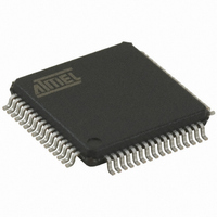
AT32UC3B0512-A2UT Atmel, AT32UC3B0512-A2UT Datasheet - Page 612

AT32UC3B0512-A2UT
Manufacturer Part Number
AT32UC3B0512-A2UT
Description
IC MCU AVR32 512K FLASH 64TQFP
Manufacturer
Atmel
Series
AVR®32 UC3r
Specifications of AT32UC3B0512-A2UT
Core Processor
AVR
Core Size
32-Bit
Speed
60MHz
Connectivity
I²C, IrDA, SPI, SSC, UART/USART, USB
Peripherals
Brown-out Detect/Reset, DMA, POR, PWM, WDT
Number Of I /o
44
Program Memory Size
512KB (512K x 8)
Program Memory Type
FLASH
Ram Size
96K x 8
Voltage - Supply (vcc/vdd)
1.65 V ~ 1.95 V
Data Converters
A/D 8x10b
Oscillator Type
Internal
Operating Temperature
-40°C ~ 85°C
Package / Case
64-TQFP, 64-VQFP
Controller Family/series
AT32UC3B
No. Of I/o's
44
Ram Memory Size
96KB
Cpu Speed
60MHz
No. Of Timers
1
Rohs Compliant
Yes
Lead Free Status / RoHS Status
Lead free / RoHS Compliant
Eeprom Size
-
Available stocks
Company
Part Number
Manufacturer
Quantity
Price
Company:
Part Number:
AT32UC3B0512-A2UT
Manufacturer:
MURATA
Quantity:
11 450
Part Number:
AT32UC3B0512-A2UT
Manufacturer:
ATMEL/爱特梅尔
Quantity:
20 000
- Current page: 612 of 692
- Download datasheet (11Mb)
27.5.3.8
32059K–03/2011
AVR_RESET
The full 16-bit counter value must be provided when starting the synch operation, or the result
will be undefined. When reading status, shifting may be terminated once the required number of
bits have been acquired.
Table 27-23. SYNC_ACCESS Details
This instruction allows a debugger or tester to directly control separate reset domains inside the
chip. The shift register contains one bit for each controllable reset domain. Setting a bit to one
resets that domain and holds it in reset. Setting a bit to zero releases the reset for that domain.
The AVR_RESET instruction can be used in the following way:
See the device specific documentation for the number of reset domains, and what these
domains are.
For any operation, all bits must be provided or the result will be undefined.
Table 27-24. AVR_RESET Details
Instructions
IR input value
IR output value
DR Size
DR input value
DR output value
Instructions
IR input value
IR output value
6. Scan in an 16-bit counter value.
7. Go to Update-DR and re-enter Select-DR Scan.
8. In Shift-DR: Scan out the busy bit, and until the busy bit clears goto 7.
9. Calculate an approximation to the internal clock speed using the elapsed time and the
10. Return to Run-Test/Idle.
1. Select the IR Scan path.
2. In Capture-IR: The IR output value is latched into the shift register.
3. In Shift-IR: The instruction register is shifted by the TCK input.
4. Return to Run-Test/Idle.
5. Select the DR Scan path.
6. In Shift-DR: Scan in the value corresponding to the reset domains the JTAG master
7. Return to Run-Test/Idle.
8. Stay in run test idle for at least 10 TCK clock cycles to let the reset propagate to the
counter value.
wants to reset into the data register.
system.
Details
10111 (0x17)
peb01
16 bits
dddddddd dddddddd
xxxxxxxx xxxxxxeb
Details
01100 (0x0C)
p0001
AT32UC3B
612
Related parts for AT32UC3B0512-A2UT
Image
Part Number
Description
Manufacturer
Datasheet
Request
R

Part Number:
Description:
DEV KIT FOR AVR/AVR32
Manufacturer:
Atmel
Datasheet:

Part Number:
Description:
INTERVAL AND WIPE/WASH WIPER CONTROL IC WITH DELAY
Manufacturer:
ATMEL Corporation
Datasheet:

Part Number:
Description:
Low-Voltage Voice-Switched IC for Hands-Free Operation
Manufacturer:
ATMEL Corporation
Datasheet:

Part Number:
Description:
MONOLITHIC INTEGRATED FEATUREPHONE CIRCUIT
Manufacturer:
ATMEL Corporation
Datasheet:

Part Number:
Description:
AM-FM Receiver IC U4255BM-M
Manufacturer:
ATMEL Corporation
Datasheet:

Part Number:
Description:
Monolithic Integrated Feature Phone Circuit
Manufacturer:
ATMEL Corporation
Datasheet:

Part Number:
Description:
Multistandard Video-IF and Quasi Parallel Sound Processing
Manufacturer:
ATMEL Corporation
Datasheet:

Part Number:
Description:
High-performance EE PLD
Manufacturer:
ATMEL Corporation
Datasheet:

Part Number:
Description:
8-bit Flash Microcontroller
Manufacturer:
ATMEL Corporation
Datasheet:

Part Number:
Description:
2-Wire Serial EEPROM
Manufacturer:
ATMEL Corporation
Datasheet:


