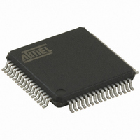
AT32UC3B0512-A2UT Atmel, AT32UC3B0512-A2UT Datasheet - Page 174

AT32UC3B0512-A2UT
Manufacturer Part Number
AT32UC3B0512-A2UT
Description
IC MCU AVR32 512K FLASH 64TQFP
Manufacturer
Atmel
Series
AVR®32 UC3r
Specifications of AT32UC3B0512-A2UT
Core Processor
AVR
Core Size
32-Bit
Speed
60MHz
Connectivity
I²C, IrDA, SPI, SSC, UART/USART, USB
Peripherals
Brown-out Detect/Reset, DMA, POR, PWM, WDT
Number Of I /o
44
Program Memory Size
512KB (512K x 8)
Program Memory Type
FLASH
Ram Size
96K x 8
Voltage - Supply (vcc/vdd)
1.65 V ~ 1.95 V
Data Converters
A/D 8x10b
Oscillator Type
Internal
Operating Temperature
-40°C ~ 85°C
Package / Case
64-TQFP, 64-VQFP
Controller Family/series
AT32UC3B
No. Of I/o's
44
Ram Memory Size
96KB
Cpu Speed
60MHz
No. Of Timers
1
Rohs Compliant
Yes
Lead Free Status / RoHS Status
Lead free / RoHS Compliant
Eeprom Size
-
Available stocks
Company
Part Number
Manufacturer
Quantity
Price
Company:
Part Number:
AT32UC3B0512-A2UT
Manufacturer:
MURATA
Quantity:
11 450
Part Number:
AT32UC3B0512-A2UT
Manufacturer:
ATMEL/爱特梅尔
Quantity:
20 000
- Current page: 174 of 692
- Download datasheet (11Mb)
17.5.1.4
17.5.1.5
17.5.2
17.5.2.1
17.5.2.2
32059K–03/2011
Advanced Operation
Inputs
Output line timings
Pull-up resistor control
Input glitch filter
responding I/O line is driven by the GPIO. When the bit is written to zero, the GPIO does not
drive the line.
The level driven on an I/O line can be determined by writing to the Output Value Register (OVR).
The level on each I/O line can be read through the Pin Value Register (PVR). This register indi-
cates the level of the I/O lines regardless of whether the lines are driven by the GPIO or by an
external component. Note that due to power saving measures, the PVR register can only be
read when GPER is written to one for the corresponding pin or if interrupt is enabled for the pin.
The figure below shows the timing of the I/O line when writing a one and a zero to OVR. The
same timing applies when performing a ‘set’ or ‘clear’ access, i.e., writing a one to the Output
Value Set Register (OVRS) or the Output Value Clear Register (OVRC). The timing of PVR is
also shown.
Figure 17-3. Output Line Timings
Each I/O line is designed with an embedded pull-up resistor. The pull-up resistor can be enabled
or disabled by writing a one or a zero to the corresponding bit in the Pull-up Enable Register
(PUER). Control of the pull-up resistor is possible whether an I/O line is controlled by a periph-
eral or the GPIO.
Optional input glitch filters can be enabled on each I/O line. When the glitch filter is enabled, a
glitch with duration of less than 1 clock cycle is automatically rejected, while a pulse with dura-
tion of 2 clock cycles or more is accepted. For pulse durations between 1 clock cycle and 2 clock
cycles, the pulse may or may not be taken into account, depending on the precise timing of its
occurrence. Thus for a pulse to be guaranteed visible it must exceed 2 clock cycles, whereas for
a glitch to be reliably filtered out, its duration must not exceed 1 clock cycle. The filter introduces
2 clock cycles of latency.
The glitch filters are controlled by the Glitch Filter Enable Register (GFER). When a bit is written
to one in GFER, the glitch filter on the corresponding pin is enabled. The glitch filter affects only
interrupt inputs. Inputs to peripherals or the value read through PVR are not affected by the
glitch filters.
Write OVR to 1
Write OVR to 0
OVR / I/O Line
CLK_GPIO
PVR
PB Access
PB Access
AT32UC3B
174
Related parts for AT32UC3B0512-A2UT
Image
Part Number
Description
Manufacturer
Datasheet
Request
R

Part Number:
Description:
DEV KIT FOR AVR/AVR32
Manufacturer:
Atmel
Datasheet:

Part Number:
Description:
INTERVAL AND WIPE/WASH WIPER CONTROL IC WITH DELAY
Manufacturer:
ATMEL Corporation
Datasheet:

Part Number:
Description:
Low-Voltage Voice-Switched IC for Hands-Free Operation
Manufacturer:
ATMEL Corporation
Datasheet:

Part Number:
Description:
MONOLITHIC INTEGRATED FEATUREPHONE CIRCUIT
Manufacturer:
ATMEL Corporation
Datasheet:

Part Number:
Description:
AM-FM Receiver IC U4255BM-M
Manufacturer:
ATMEL Corporation
Datasheet:

Part Number:
Description:
Monolithic Integrated Feature Phone Circuit
Manufacturer:
ATMEL Corporation
Datasheet:

Part Number:
Description:
Multistandard Video-IF and Quasi Parallel Sound Processing
Manufacturer:
ATMEL Corporation
Datasheet:

Part Number:
Description:
High-performance EE PLD
Manufacturer:
ATMEL Corporation
Datasheet:

Part Number:
Description:
8-bit Flash Microcontroller
Manufacturer:
ATMEL Corporation
Datasheet:

Part Number:
Description:
2-Wire Serial EEPROM
Manufacturer:
ATMEL Corporation
Datasheet:


