ATTINY44-15MZ Atmel, ATTINY44-15MZ Datasheet - Page 102
ATTINY44-15MZ
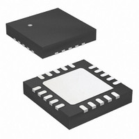
Manufacturer Part Number
ATTINY44-15MZ
Description
MCU AVR 4K FLASH 15MHZ 20-QFN
Manufacturer
Atmel
Series
AVR® ATtinyr
Datasheet
1.ATTINY44-15MZ.pdf
(225 pages)
Specifications of ATTINY44-15MZ
Package / Case
20-QFN Exposed Pad
Voltage - Supply (vcc/vdd)
2.7 V ~ 5.5 V
Operating Temperature
-40°C ~ 125°C
Speed
16MHz
Number Of I /o
12
Eeprom Size
256 x 8
Core Processor
AVR
Program Memory Type
FLASH
Ram Size
256 x 8
Program Memory Size
4KB (4K x 8)
Data Converters
A/D 8x10b
Oscillator Type
Internal
Peripherals
Brown-out Detect/Reset, POR, PWM, WDT
Connectivity
USI
Core Size
8-Bit
Processor Series
ATTINY4x
Core
AVR8
Data Bus Width
8 bit
Data Ram Size
256 B
Interface Type
SPI, UART
Maximum Clock Frequency
16 MHz
Number Of Programmable I/os
12
Number Of Timers
2
Maximum Operating Temperature
+ 85 C
Mounting Style
SMD/SMT
3rd Party Development Tools
EWAVR, EWAVR-BL
Development Tools By Supplier
ATAVRDRAGON, ATSTK500, ATSTK600, ATAVRISP2, ATAVRONEKIT
Minimum Operating Temperature
- 40 C
On-chip Adc
10 bit, 8 Channel
Lead Free Status / RoHS Status
Lead free / RoHS Compliant
Available stocks
Company
Part Number
Manufacturer
Quantity
Price
Company:

Part Number:
ATTINY44-15MZ
Manufacturer:
ATMEL
Quantity:
1 000
Part Number:
ATTINY44-15MZ
Manufacturer:
ATMEL/爱特梅尔
Quantity:
20 000


14.8
102
Compare Match Output Unit
Atmel ATtiny24/44/84 [Preliminary]
Be aware that the COM1x1:0 bits are not double buffered together with the compare value.
Changing the COM1x1:0 bits will take effect immediately.
The Compare Output mode (COM1x1:0) bits have two functions. The Waveform Generator
uses the COM1x1:0 bits for defining the Output Compare (OC1x) state at the next compare
match. Secondly the COM1x1:0 bits control the OC1x pin output source.
102
registers, I/O bits, and I/O pins in the figure are shown in bold. Only the parts of the general I/O
port control registers (DDR and PORT) that are affected by the COM1x1:0 bits are shown.
When referring to the OC1x state, the reference is for the internal OC1x register, not the OC1x
pin. If a system reset occurs, the OC1x register is reset to "0".
Figure 14-5. Compare Match Output Unit, Schematic
The general I/O port function is overridden by the Output Compare (OC1x) from the Waveform
Generator if either of the COM1x1:0 bits are set. However, the OC1x pin direction (input or
output) is still controlled by the Data Direction Register (DDR) for the port pin. The Data Direc-
tion Register bit for the OC1x pin (DDR_OC1x) must be set as output before the OC1x value is
visible on the pin. The port override function is generally independent of the Waveform Gener-
ation mode, but there are some exceptions. See
113
The design of the Output Compare pin logic allows initialization of the OC1x state before the
output is enabled. Note that some COM1x1:0 bit settings are reserved for certain modes of
operation. See
The COM1x1:0 bits have no effect on the Input Capture unit.
and
shows a simplified schematic of the logic affected by the COM1x1:0 bit settings. The I/O
COMnx1
COMnx0
FOCnx
clk
I/O
Table 14-3 on page 114
“Register Description” on page 113
Waveform
Generator
for details.
D
D
D
PORT
DDR
OCnx
Q
Q
Q
Table 14-1 on page
1
0
113,
Figure 14-5 on page
Table 14-2 on page
7701E–AVR–02/11
OCnx
Pin
Related parts for ATTINY44-15MZ
Image
Part Number
Description
Manufacturer
Datasheet
Request
R

Part Number:
Description:
Manufacturer:
Atmel Corporation
Datasheet:
Part Number:
Description:
Manufacturer:
Atmel Corporation
Datasheet:

Part Number:
Description:
IC MCU AVR 4K FLASH 20MHZ 20-QFN
Manufacturer:
Atmel
Datasheet:

Part Number:
Description:
IC MCU AVR 4K FLASH 20MHZ 14SOIC
Manufacturer:
Atmel
Datasheet:

Part Number:
Description:
MCU AVR 4KB FLASH 20MHZ 14SOIC
Manufacturer:
Atmel
Datasheet:
Part Number:
Description:
MCU AVR 4KB FLASH 20MHZ 20QFN
Manufacturer:
Atmel
Datasheet:
Part Number:
Description:
IC MCU AVR 4K FLASH 15MHZ 14SOIC
Manufacturer:
Atmel
Datasheet:

Part Number:
Description:
IC MCU AVR 4K FLASH 20MHZ 14-DIP
Manufacturer:
Atmel
Datasheet:
Part Number:
Description:
Manufacturer:
Atmel Corporation
Datasheet:
Part Number:
Description:
Microcontrollers (MCU) 512B FL 32B SRAM TIMER ATTINY4 12MHz
Manufacturer:
Atmel
Part Number:
Description:
IC MCU AVR 512B FLASH SOT-23-6
Manufacturer:
Atmel
Datasheet:

Part Number:
Description:
IC MCU AVR 512B FLASH SOT-23-6
Manufacturer:
Atmel
Datasheet: