ATTINY44-15MZ Atmel, ATTINY44-15MZ Datasheet - Page 101
ATTINY44-15MZ
Manufacturer Part Number
ATTINY44-15MZ
Description
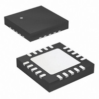
MCU AVR 4K FLASH 15MHZ 20-QFN
Manufacturer
Atmel
Series
AVR® ATtinyr
Datasheet
1.ATTINY44-15MZ.pdf
(225 pages)
Specifications of ATTINY44-15MZ
Package / Case
20-QFN Exposed Pad
Voltage - Supply (vcc/vdd)
2.7 V ~ 5.5 V
Operating Temperature
-40°C ~ 125°C
Speed
16MHz
Number Of I /o
12
Eeprom Size
256 x 8
Core Processor
AVR
Program Memory Type
FLASH
Ram Size
256 x 8
Program Memory Size
4KB (4K x 8)
Data Converters
A/D 8x10b
Oscillator Type
Internal
Peripherals
Brown-out Detect/Reset, POR, PWM, WDT
Connectivity
USI
Core Size
8-Bit
Processor Series
ATTINY4x
Core
AVR8
Data Bus Width
8 bit
Data Ram Size
256 B
Interface Type
SPI, UART
Maximum Clock Frequency
16 MHz
Number Of Programmable I/os
12
Number Of Timers
2
Maximum Operating Temperature
+ 85 C
Mounting Style
SMD/SMT
3rd Party Development Tools
EWAVR, EWAVR-BL
Development Tools By Supplier
ATAVRDRAGON, ATSTK500, ATSTK600, ATAVRISP2, ATAVRONEKIT
Minimum Operating Temperature
- 40 C
On-chip Adc
10 bit, 8 Channel
Lead Free Status / RoHS Status
Lead free / RoHS Compliant
Available stocks
Company
Part Number
Manufacturer
Quantity
Price
Company:

Part Number:
ATTINY44-15MZ
Manufacturer:
ATMEL
Quantity:
1 000
Part Number:
ATTINY44-15MZ
Manufacturer:
ATMEL/爱特梅尔
Quantity:
20 000


14.7.1
14.7.2
14.7.3
7701E–AVR–02/11
Force Output Compare
Compare Match Blocking by TCNT1 Write
Using the Output Compare Unit
The OCR1x register is double buffered when using any of the twelve pulse width modulation
(PWM) modes. For the normal and clear timer on compare (CTC) modes of operation, the
double buffering is disabled. The double buffering synchronizes the update of the OCR1x
compare register to either top or bottom of the counting sequence. The synchronization pre-
vents the occurrence of odd-length, non-symmetrical PWM pulses, thereby making the output
glitch-free.
The OCR1x register access may seem complex, but this is not the case. When the double
buffering is enabled, the CPU has access to the OCR1x buffer register, and if double buffering
is disabled the CPU will access the OCR1x directly. The content of the OCR1x (buffer or com-
pare) register is changed only by a write operation (the timer/counter does not update this
register automatically as it does for the TCNT1 and ICR1 registers). Therefore, OCR1x is not
read via the high byte temporary register (TEMP). However, it is a good practice to read the
low byte first, as when accessing other 16-bit registers. Writing the OCR1x registers must be
done via the TEMP register because the compare of all 16 bits is done continuously. The high
byte (OCR1xH) has to be written first. When the high byte I/O location is written by the CPU,
the TEMP register will be updated by the value written. Then when the low byte (OCR1xL) is
written to the lower eight bits, the high byte will be copied into the upper 8-bits of either the
OCR1x buffer or the OCR1x compare register in the same system clock cycle.
For more information of how to access the 16-bit registers, refer to
ters” on page
In non-PWM waveform generation modes, the match output of the comparator can be forced
by writing a logical one to the Force Output Compare (1x) bit. Forcing compare match will not
set the OCF1x flag or reload/clear the timer, but the OC1x pin will be updated as if a real com-
pare match had occurred (the COM11:0 bit settings define whether the OC1x pin is set,
cleared or toggled).
All CPU writes to the TCNT1 Register will block any compare match that occurs in the next
timer clock cycle, even when the timer is stopped. This feature allows OCR1x to be initialized
to the same value as TCNT1 without triggering an interrupt when the Timer/Counter clock is
enabled.
Because writing TCNT1 in any mode of operation will block all compare matches for one timer
clock cycle, there are risks involved in changing TCNT1 when using any of the output compare
channels, independent of whether the timer/counter is running or not. If the value written to
TCNT1 equals the OCR1x value, the compare match will be missed, resulting in incorrect
waveform generation. Do not write the TCNT1 equal to top in PWM modes with variable top
values. The compare match for the top will be ignored, and the counter will continue to
0xFFFF. Similarly, do not write the TCNT1 value equal to bottom when the counter is
down-counting.
The setup of the OC1x should be performed before setting the data direction register for the
port pin to output. The easiest way of setting the OC1x value is to use the force output com-
pare (1x) strobe bits in normal mode. The OC1x register keeps its value even when changing
between waveform generation modes.
94.
Atmel ATtiny24/44/84 [Preliminary]
“Accessing 16-bit Regis-
101
Related parts for ATTINY44-15MZ
Image
Part Number
Description
Manufacturer
Datasheet
Request
R

Part Number:
Description:
Manufacturer:
Atmel Corporation
Datasheet:
Part Number:
Description:
Manufacturer:
Atmel Corporation
Datasheet:

Part Number:
Description:
IC MCU AVR 4K FLASH 20MHZ 20-QFN
Manufacturer:
Atmel
Datasheet:

Part Number:
Description:
IC MCU AVR 4K FLASH 20MHZ 14SOIC
Manufacturer:
Atmel
Datasheet:

Part Number:
Description:
MCU AVR 4KB FLASH 20MHZ 14SOIC
Manufacturer:
Atmel
Datasheet:
Part Number:
Description:
MCU AVR 4KB FLASH 20MHZ 20QFN
Manufacturer:
Atmel
Datasheet:
Part Number:
Description:
IC MCU AVR 4K FLASH 15MHZ 14SOIC
Manufacturer:
Atmel
Datasheet:

Part Number:
Description:
IC MCU AVR 4K FLASH 20MHZ 14-DIP
Manufacturer:
Atmel
Datasheet:
Part Number:
Description:
Manufacturer:
Atmel Corporation
Datasheet:
Part Number:
Description:
Microcontrollers (MCU) 512B FL 32B SRAM TIMER ATTINY4 12MHz
Manufacturer:
Atmel
Part Number:
Description:
IC MCU AVR 512B FLASH SOT-23-6
Manufacturer:
Atmel
Datasheet:

Part Number:
Description:
IC MCU AVR 512B FLASH SOT-23-6
Manufacturer:
Atmel
Datasheet: