M30833FJFP#U5 Renesas Electronics America, M30833FJFP#U5 Datasheet - Page 525
M30833FJFP#U5
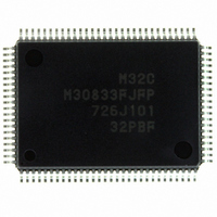
Manufacturer Part Number
M30833FJFP#U5
Description
IC M32C/83 MCU FLASH 100QFP
Manufacturer
Renesas Electronics America
Series
M16C™ M32C/80r
Datasheets
1.M3087BFLGPU3.pdf
(364 pages)
2.M30833FJGPU3.pdf
(96 pages)
3.M30833FJGPU3.pdf
(529 pages)
Specifications of M30833FJFP#U5
Core Processor
M32C/80
Core Size
16/32-Bit
Speed
32MHz
Connectivity
CAN, I²C, IEBus, SIO, UART/USART
Peripherals
DMA, WDT
Number Of I /o
85
Program Memory Size
512KB (512K x 8)
Program Memory Type
FLASH
Ram Size
31K x 8
Voltage - Supply (vcc/vdd)
3 V ~ 5.5 V
Data Converters
A/D 26x10b; D/A 2x8b
Oscillator Type
Internal
Operating Temperature
-20°C ~ 85°C
Package / Case
100-QFP
For Use With
R0K330879S001BE - KIT DEV RSK M32C/87R0K330879S000BE - KIT DEV RSK M32C/87
Lead Free Status / RoHS Status
Lead free / RoHS Compliant
Eeprom Size
-
Available stocks
Company
Part Number
Manufacturer
Quantity
Price

Part Number:
M30833FJFP#U5M30833FJFP#U3
Manufacturer:
Renesas Electronics America
Quantity:
135
Part Number:
M30833FJFP#U5M30833FJFP#U3
Manufacturer:
Renesas Electronics America
Quantity:
10 000


Rev.
REVISION HISTORY
Date
84-85
Page
109
110
113
115
119
48
49
50
52
54
58
67
68
71
74
75
76
78
80
81
82
83
85
86
97
98
Processor Mode
• Chapter Note added
• Figure 6.1 PM0 Register Note 9 added
• Figure 6.2 PM1 Register Note 6 added
Bus
• Chapter note added
• Figure 7.1 DS Register Note 2 added
• Table 7.2 Processor Mode and Port Function Note 3 modified
• Table 7.3 WCR Register Note 3 added
Clock Generation Circuit
• Figure 8.2 CM0 Register Function of the CM07 bit modified
• Figure 8.3 CM1 Register Note mark position changed
• Figure 8.6 TCSPR and CPSRF Register Note 2 added for TCSPR register
• Figure 8.9 Main Clock Circuit Connection modified
• Figure 8.10 Sub Clock Connection Circuit modified
• 8.1.3.2 How to Use Oscillation Stop Detect Function partially modified
• Figure 8.12 External Circuit with PLL Frequency Synthesizer modified
• Table 8.5 BLCK/CLKOUT Pin in Memory Expansion Mode and
• 8.5.1 Normal Operation Mode Description partially modified
• 8.5.2 Wait Mode modified
• Table 8.6 Pin States in Wait Mode Note 2 added
• 8.5.3 Stop Mode modified
• Table 8.8 Pin Status in Stop Mode Note 2 added
• Figure 8.14 Status Transition in Wait Mode and Stop Mode The mode
Interrupts
• Figure 10.4 Interrupt Control Register (2) Note mark position changed
• Figure 10.5 RLVL Register Note 3 modified
• Figure 10.14 IIO0IR to IIO11IR Registers partially modified
• Figure 10.15 IIO0IE to IIO11IE Registers partially modified
Watchdog Timer
• Figure 11.3 CM0 Register Function of the CM07 bit modified
DMAC
• Table 12.1 DMAC Specifications Specification of DMA Transfer Cycles
• Figure 12.4 DCT0 to DCT3 Registers Notes 3 and 4 modified; DRC0 to DRC3
Microprocessor Mode Note 4 added
between stop mode and low-speed mode, low-power consumption mode
changed; Note 2 deleted
partially modified
Registers Notes 2 and 4 modified
M32C/83 GROUP (M32C/83, M32C/83T) Hardware Manual
C-12
Description
Summary
Related parts for M30833FJFP#U5
Image
Part Number
Description
Manufacturer
Datasheet
Request
R

Part Number:
Description:
KIT STARTER FOR M16C/29
Manufacturer:
Renesas Electronics America
Datasheet:

Part Number:
Description:
KIT STARTER FOR R8C/2D
Manufacturer:
Renesas Electronics America
Datasheet:

Part Number:
Description:
R0K33062P STARTER KIT
Manufacturer:
Renesas Electronics America
Datasheet:

Part Number:
Description:
KIT STARTER FOR R8C/23 E8A
Manufacturer:
Renesas Electronics America
Datasheet:

Part Number:
Description:
KIT STARTER FOR R8C/25
Manufacturer:
Renesas Electronics America
Datasheet:

Part Number:
Description:
KIT STARTER H8S2456 SHARPE DSPLY
Manufacturer:
Renesas Electronics America
Datasheet:

Part Number:
Description:
KIT STARTER FOR R8C38C
Manufacturer:
Renesas Electronics America
Datasheet:

Part Number:
Description:
KIT STARTER FOR R8C35C
Manufacturer:
Renesas Electronics America
Datasheet:

Part Number:
Description:
KIT STARTER FOR R8CL3AC+LCD APPS
Manufacturer:
Renesas Electronics America
Datasheet:
Part Number:
Description:
KIT STARTER FOR RX610
Manufacturer:
Renesas Electronics America
Datasheet:

Part Number:
Description:
KIT STARTER FOR R32C/118
Manufacturer:
Renesas Electronics America
Datasheet:

Part Number:
Description:
KIT DEV RSK-R8C/26-29
Manufacturer:
Renesas Electronics America
Datasheet:

Part Number:
Description:
KIT STARTER FOR SH7124
Manufacturer:
Renesas Electronics America
Datasheet:

Part Number:
Description:
KIT STARTER FOR H8SX/1622
Manufacturer:
Renesas Electronics America
Datasheet:

Part Number:
Description:
KIT DEV FOR SH7203
Manufacturer:
Renesas Electronics America
Datasheet: