M30833FJFP#U5 Renesas Electronics America, M30833FJFP#U5 Datasheet - Page 520
M30833FJFP#U5
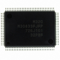
Manufacturer Part Number
M30833FJFP#U5
Description
IC M32C/83 MCU FLASH 100QFP
Manufacturer
Renesas Electronics America
Series
M16C™ M32C/80r
Datasheets
1.M3087BFLGPU3.pdf
(364 pages)
2.M30833FJGPU3.pdf
(96 pages)
3.M30833FJGPU3.pdf
(529 pages)
Specifications of M30833FJFP#U5
Core Processor
M32C/80
Core Size
16/32-Bit
Speed
32MHz
Connectivity
CAN, I²C, IEBus, SIO, UART/USART
Peripherals
DMA, WDT
Number Of I /o
85
Program Memory Size
512KB (512K x 8)
Program Memory Type
FLASH
Ram Size
31K x 8
Voltage - Supply (vcc/vdd)
3 V ~ 5.5 V
Data Converters
A/D 26x10b; D/A 2x8b
Oscillator Type
Internal
Operating Temperature
-20°C ~ 85°C
Package / Case
100-QFP
For Use With
R0K330879S001BE - KIT DEV RSK M32C/87R0K330879S000BE - KIT DEV RSK M32C/87
Lead Free Status / RoHS Status
Lead free / RoHS Compliant
Eeprom Size
-
Available stocks
Company
Part Number
Manufacturer
Quantity
Price

Part Number:
M30833FJFP#U5M30833FJFP#U3
Manufacturer:
Renesas Electronics America
Quantity:
135
Part Number:
M30833FJFP#U5M30833FJFP#U3
Manufacturer:
Renesas Electronics America
Quantity:
10 000


Rev.
REVISION HISTORY
Date
182 to 219 • Tables 16.2, 16.7, 16.12, 16.19, 16.24, and 16.34 Registers to be Used and
197, 198 • Tables 16.14 to 16.16 Pin Settings in I
Page
169
170
173
175
176
181
183
184
188
189
190
192
195
196
200
203
204
208
210
213
219
• Figure 15.8 Triangular Wave Modulation Operation modified
• Figure 15.9 Sawtooth Wave Modulation Operation modified
Serial I/O
• Figure 16.2 U0TB to U4TB Registers and U0RB to U4RB Registers Note 3
• Figure 16.4 UiC0 Register Note 3 added to UFORM bit
• Figure 16.5 UiC1 Register Note 2 added to UiLCH bit; Note 1 added to
• Table 16.1 Clock Synchrnous Serial I/O Mode Specifications Explanation of
• Table 16.3 Pin Settings in Clock Synchronous Serial I/O Mode (1) revised
• Figure 16.10 Transmit and Receive Operation modified
• Table 16.7 Registers to be Used and Settings in UART Mode Function of the
• Table 16.8 Pin Settings in UART (1) revised
• Figure 16.14 Transmit Operation modified
• Figure 16.17 Serial Data Logic Inverse modified
• Table 16.12 Registers to be Used and Settings (I
• Table 16.13 I
• 16.3.4 Transfer Clock revised
• Table 16.19 Registers to be Used and Settings in Special Mode 2 Functions
• Table 16.20 Pin Settings in Special Mode 2 (1) revised
• Table 16.21 Pin Settings in Special Mode 2 (2) revised
• Table 16.22 Pin Settings in Special Mode 2 (3) revised
• Table 16.23 GCI Mode Specifications Explanations of Transmit/Receive Start
• Table 16.25 Pin Settings in GCI Mode (1) revised
• Table 16.26 Pin Settings in GCI Mode (2) revised
• Table 16.27 Pin Settings in GCI Mode (3) revised
• Table 16.31 Pin Settings in IE Mode (2) revised
• Table 16.32 Pin Settings in IE Mode (3) revised
• Figure 16.29 SIM Interface Operation modified
added to U0RB to U4RB registers
SCLKSTPB (UiERE) bit
CLK Polarity in Selectable Functions revised
Settings Points of reference deleted
UiERE bit in the UiC1 register modified
master and slave indicated separately
changed to “P6
of the UFORM bit in the UiC0 register and the UiRRM bit in the UiC1 register
modified
Conditions revised
M32C/83 GROUP (M32C/83, M32C/83T) Hardware Manual
2
C Mode Functions “P6
1
, P6
5
C-7
, P7
2
, P9
Description
0
, P9
Summary
5
Pin Functions”
2
1
C Mode modified
, P6
5
, P7
2
2
C Mode) Setting values for
, P9
0
, P7
5
Pin Functions”
Related parts for M30833FJFP#U5
Image
Part Number
Description
Manufacturer
Datasheet
Request
R

Part Number:
Description:
KIT STARTER FOR M16C/29
Manufacturer:
Renesas Electronics America
Datasheet:

Part Number:
Description:
KIT STARTER FOR R8C/2D
Manufacturer:
Renesas Electronics America
Datasheet:

Part Number:
Description:
R0K33062P STARTER KIT
Manufacturer:
Renesas Electronics America
Datasheet:

Part Number:
Description:
KIT STARTER FOR R8C/23 E8A
Manufacturer:
Renesas Electronics America
Datasheet:

Part Number:
Description:
KIT STARTER FOR R8C/25
Manufacturer:
Renesas Electronics America
Datasheet:

Part Number:
Description:
KIT STARTER H8S2456 SHARPE DSPLY
Manufacturer:
Renesas Electronics America
Datasheet:

Part Number:
Description:
KIT STARTER FOR R8C38C
Manufacturer:
Renesas Electronics America
Datasheet:

Part Number:
Description:
KIT STARTER FOR R8C35C
Manufacturer:
Renesas Electronics America
Datasheet:

Part Number:
Description:
KIT STARTER FOR R8CL3AC+LCD APPS
Manufacturer:
Renesas Electronics America
Datasheet:
Part Number:
Description:
KIT STARTER FOR RX610
Manufacturer:
Renesas Electronics America
Datasheet:

Part Number:
Description:
KIT STARTER FOR R32C/118
Manufacturer:
Renesas Electronics America
Datasheet:

Part Number:
Description:
KIT DEV RSK-R8C/26-29
Manufacturer:
Renesas Electronics America
Datasheet:

Part Number:
Description:
KIT STARTER FOR SH7124
Manufacturer:
Renesas Electronics America
Datasheet:

Part Number:
Description:
KIT STARTER FOR H8SX/1622
Manufacturer:
Renesas Electronics America
Datasheet:

Part Number:
Description:
KIT DEV FOR SH7203
Manufacturer:
Renesas Electronics America
Datasheet: